Magnetoresistive effect element, thin-film magnetic head with the element and manufacturing method of the head

a technology of magnetic head and element, which is applied in the direction of manufacturing head surface, instruments, manufacturing tools, etc., can solve the problems of reducing affecting the reading performance of the guide, and a possibility of a degradation of the reading performance or a breakdown of the element, so as to reduce the capacitance

Inactive Publication Date: 2007-06-07
TDK CORPARATION
View PDF5 Cites 15 Cited by
  • Summary
  • Abstract
  • Description
  • Claims
  • Application Information

AI Technical Summary

Benefits of technology

[0013] Therefore, it is an object of the present invention to provide an MR effect element that can obtain the sufficient back flux-guide effect under the condition of reducing the capacitance between t

Problems solved by technology

Currently, a serious problem occurs in the CIP structure that an insufficient insulation is likely to occur between the MR effect multilayer and magnetic shield layers due to narrowing the read-gap corresponding to higher density recording.
However, the insulating layer sandwitched between the upper and lower electrode layers generates a corresponding capacitance which has a possibility to cause a degradation of the reading performance or a breakdown of the element through the influence of disturbance noise or electrostatic discharge (ESD) phenomenon, as shown, for example, Japanese patent Publication No. 2005-50418A.
However, a conventional structure having the above described back flu

Method used


Image

  • Magnetoresistive effect element, thin-film magnetic head with the element and manufacturing method of the head
  • Magnetoresistive effect element, thin-film magnetic head with the element and manufacturing method of the head
  • Magnetoresistive effect element, thin-film magnetic head with the element and manufacturing method of the head

Examples


Embodiment Construction

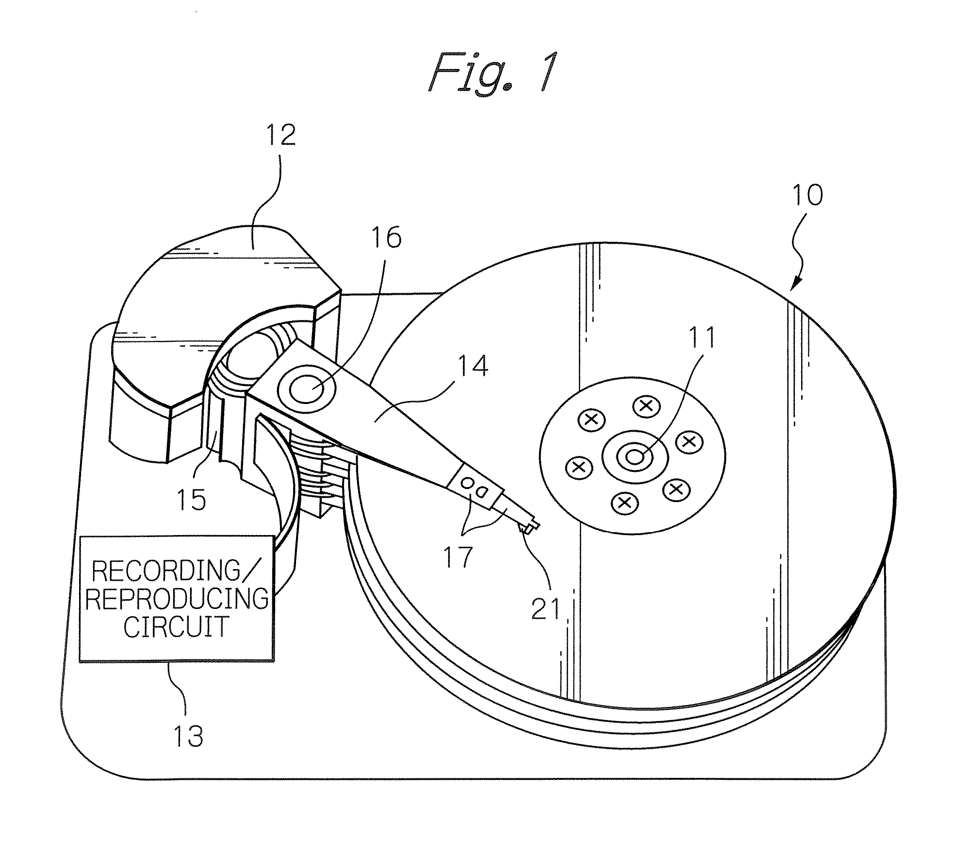
[0051]FIG. 1 shows a perspective view schematically illustrating a major portion of an embodiment of the magnetic disk drive apparatus according to the present invention.

[0052] In FIG. 1, reference numeral 10 indicates a plurality of magnetic disks rotating around a rotational axis of a spindle motor 11, 12 indicates an assembly carriage device for positioning a thin-film magnetic head (slider) 21 on a track, and 13 indicates a recording / reproducing circuit for controlling read / write operations of the thin-film magnetic head, respectively.

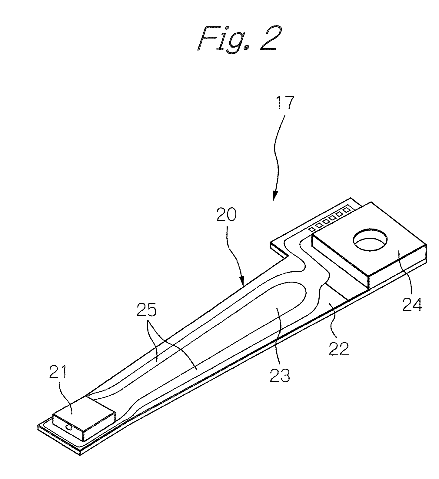
[0053] The assembly carriage device 12 is provided with a plurality of drive arms 14. These drive arms 14 are rotatable around a pivot bearing axis 16 by means of a voice coil motor (VCM) 15 and stacked in the direction along this axis 16. An HGA 17 is provided on the end portion of each drive arm 14. The thin-film magnetic head 21 is mounted on each HGA 17 in such a way as to face the surface of each magnetic disk 10. The each number of the magn...


PUM

PropertyMeasurementUnit
Angleaaaaaaaaaa
Angleaaaaaaaaaa
Distanceaaaaaaaaaa

Abstract

An MR effect element that can obtain the sufficient back flux-guide effect under the condition of reducing the capacitance between the upper and lower electrode layers is provided. The element comprises: an MR effect multilayer provided on the lower electrode layer; an insulating layer surrounding a rear side surface and side surfaces opposed to each other in track width direction of the MR effect multilayer; and an upper electrode layer provided on the MR effect multilayer and the insulating layer, the insulating layer having a concave portion filled with a portion of the upper electrode layer, the concave portion positioned near the rear side surface of the MR effect multilayer, and a bottom point of a concave of the concave portion positioned at the same level or a lower level in stacking direction compared to an upper surface of the free layer.

Description

PRIORITY CLAIM [0001] This application claims priority from Japanese patent application No. 2005-349359, filed on Dec. 2, 2005, which is incorporated herein by reference. BACKGROUND OF THE INVENTION [0002] 1. Field of the Invention [0003] The present invention relates to a magnetoresistive (MR) effect element for detecting external magnetic fields such as signal fields and showing the resistance change corresponding to the field intensity, a thin-film magnetic head having the MR effect element, a head gimbal assembly (HGA) having the thin-film magnetic head and a magnetic disk drive apparatus having the HGA. Further, the present invention relates to a manufacturing method of a thin-film magnetic head wafer and a thin-film magnetic head having the MR effect element. [0004] 2. Description of the Related Art [0005] Responding to larger capacity storage and further miniaturization of a magnetic disk drive apparatus in recent days, a giant magnetoresistive (GMR) head is being aggressivel...

Claims


Application Information

Patent Timeline
IPC IPC(8): G11B5/127G11B5/33
CPCB82Y10/00B82Y25/00G11B5/3906G11B5/3909Y10T29/49052Y10T29/49048Y10T29/49043Y10T29/49046Y10T29/49032G11B2005/3996
Inventor KANAYA, TAKAYASUSATO, KAZUKI
Owner TDK CORPARATION
Why Eureka
Try Eureka