Active-matrix liquid crystal display

a liquid crystal display and active matrix technology, applied in non-linear optics, instruments, optics, etc., can solve the problems of excessive excessive power consumption or the size of the drive circuit, and the vertical smear is extending along the video signal line on the display surface, so as to prevent the load on the drive circuit from increasing, reduce the capacitance between the shield electrode and the video signal line, and minimize the vertical smear

Inactive Publication Date: 2005-10-13
PANASONIC LIQUID CRYSTAL DISPLAY CO LTD +1
View PDF9 Cites 14 Cited by
  • Summary
  • Abstract
  • Description
  • Claims
  • Application Information

AI Technical Summary

Benefits of technology

[0019] In accordance with the first aspect of the present invention, because the video signal lines and the reference electrodes adjacent to the video signal lines, both formed on one of the transparent substrates, are completely superimposed, in plan view, by the shield electrode formed on the other transparent substrate, unwanted electric lines of force generated by the video signal lines are terminated at the shield electrode and the reference electrodes adjacent to the video signal lines, thus preventing the electric field between the display electrodes and the reference electrodes from varying depending on the video signal, and greatly minimizing the vertical smear.
[0020] Further, because the shield electrodes are formed on the substrate opposite to the video signal lines, the shield electrodes and the video signal lines are spaced more from each other by the thickness of the liquid crystal layer, so that the capacitance between the shield electrodes and the video signal lines is reduced. This prevents the load on the drive circuit from increasing, minimizes power consumption and reduces the size of the drive circuit.
[0021] In accordance with the second aspect of the present invention, because the video signal lines for allowing the display electrodes to function and the reference signal lines connected with the reference electrodes are formed to completely overlap each other, when seen in plan view, the effective pixel areas can be increased, thus improving the so-called aperture ratio.
[0022] Further, because the reference electrodes are so formed as to be electrically connected to the light shielding layer having apertures only at the pixel areas, a voltage is applied through a low resistance to the reference electrode in each pixel area. As a result, the reference signal waveforms can be prevented from becoming dull, thus minimizing what is generally called a brightness gradient and the horizontal smear.
[0023] Furthermore, the third aspect of the present invention has the features of the first and second aspects combined and can reduce the reflectance of the liquid crystal display device.

Problems solved by technology

It has been pointed out that liquid crystal display devices of this configuration, however, have a problem in that an undesired electric field produced from the video signal line changes the electric field between the display electrodes and the reference electrodes, causing so-called vertical smear extending along the video signal line on the display surface.
Liquid crystal display devices thus structured, however, have a problem in that, because the shield electrode is provided on the same substrate, the capacitance between the shield electrode and the signal electrode is large, the load on the drive circuit becomes too heavy, and the power consumption or the size of the drive circuit becomes too large.
Liquid crystal display devices thus constructed have another problem in that, because opaque electrodes are formed like a comb, the percentage of the pixel area occupied by the opaque metal is high, and so the aperture ratio cannot be increased.
Further, because a voltage is applied to the reference electrodes formed in individual pixel areas through common stripe-shaped reference signal lines extending in a row or column direction, the waveform of the applied voltage becomes dull from the signal supply portions of the reference signal lines toward the far ends of the reference signal lines, with the result that a brightness gradient or so-called horizontal smear occurs with the reference signal lines on the display surface.

Method used


Image

  • Active-matrix liquid crystal display
  • Active-matrix liquid crystal display
  • Active-matrix liquid crystal display

Examples


embodiment 1

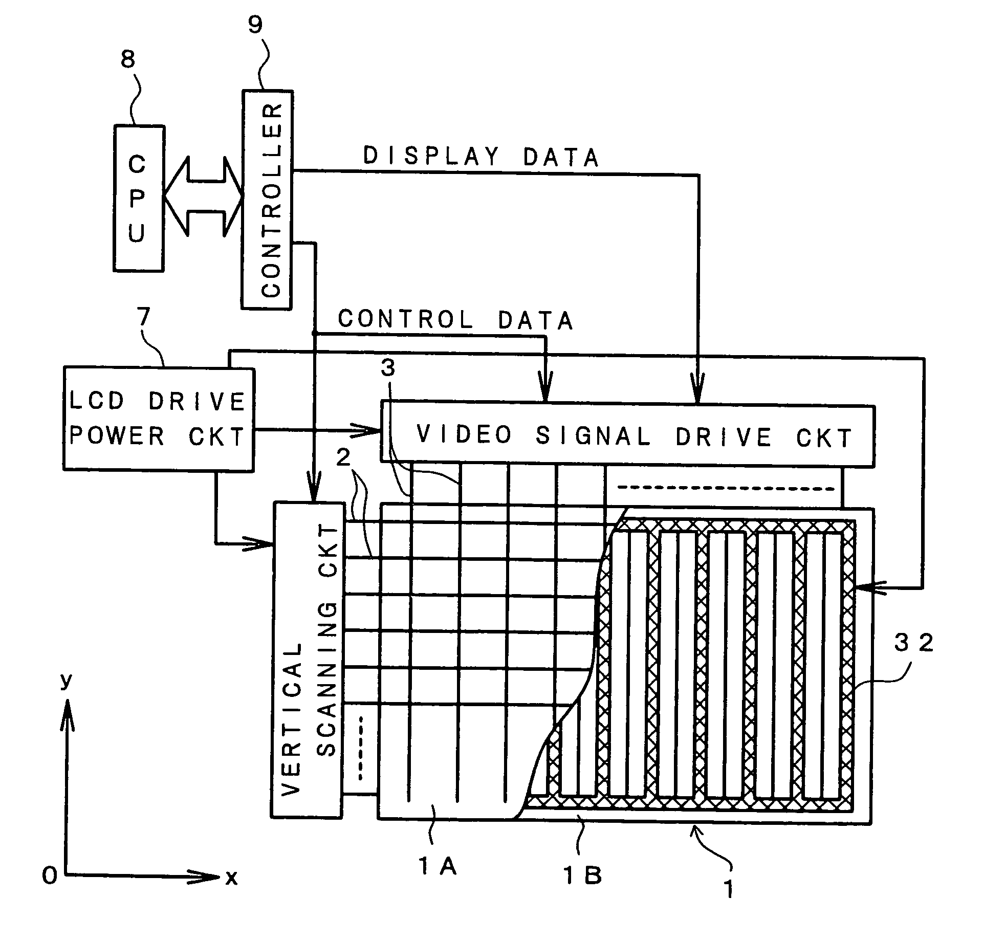
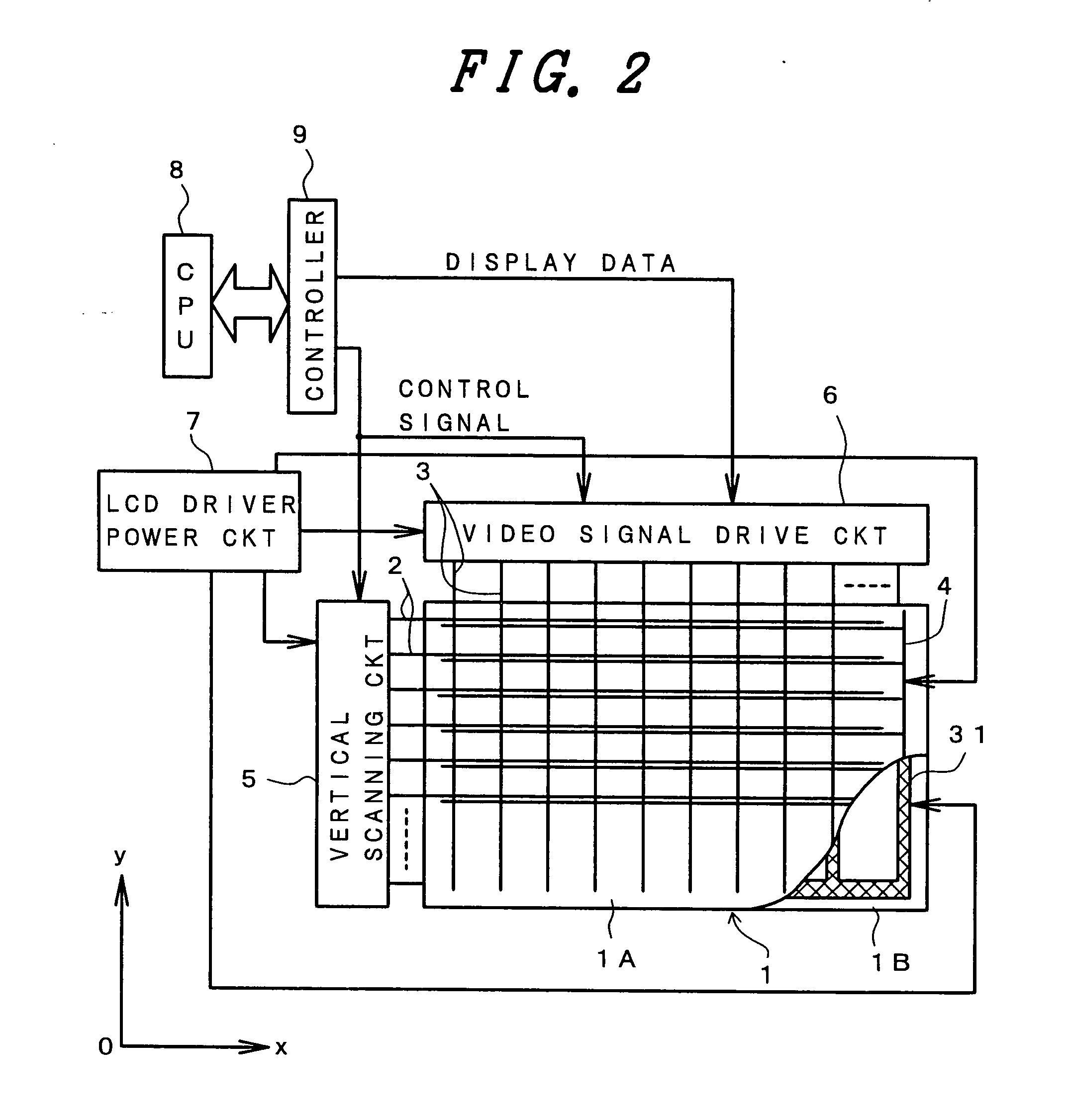
[0056]FIG. 2 is a diagram showing the configuration of one Embodiment of the liquid crystal display device of the present invention and its peripheral circuits.

[0057] In the figure, liquid crystal display device 1 has as its enclosure a transparent substrate 1A and a transparent substrate 1B with a liquid crystal layer interposed therebetween. On the surface of the transparent substrate 1A, which is a so-called lower substrate, on the liquid crystal layer side, are formed scan signal lines 2 and reference signal lines 4 that extend in the x direction in the figure and are parallelly arranged in the y direction. The scan signal lines 2 and the reference signal lines 4 are arranged alternately such that a first reference signal line 4 is provided close to a first scan signal line 2 in the (−) y direction, a second scan signal line 2 is greatly spaced from the first reference signal line 4 in the (−) y direction, a second reference signal line 4 is provided close to the second scan si...

embodiment 2

[0090] A second embodiment will be described centering on its differences from Embodiment 1.

[0091]FIG. 14 is a schematic diagram corresponding to FIG. 2. what differs from the configuration of FIG. 2 is, first, that the reference signal lines 4 and the reference electrodes 14 are not formed on the lower substrate 1B. Hence, instead of the storage capacitor Cstg used in Embodiment 1, an additional capacitor Cadd is provided in each pixel (These are not shown).

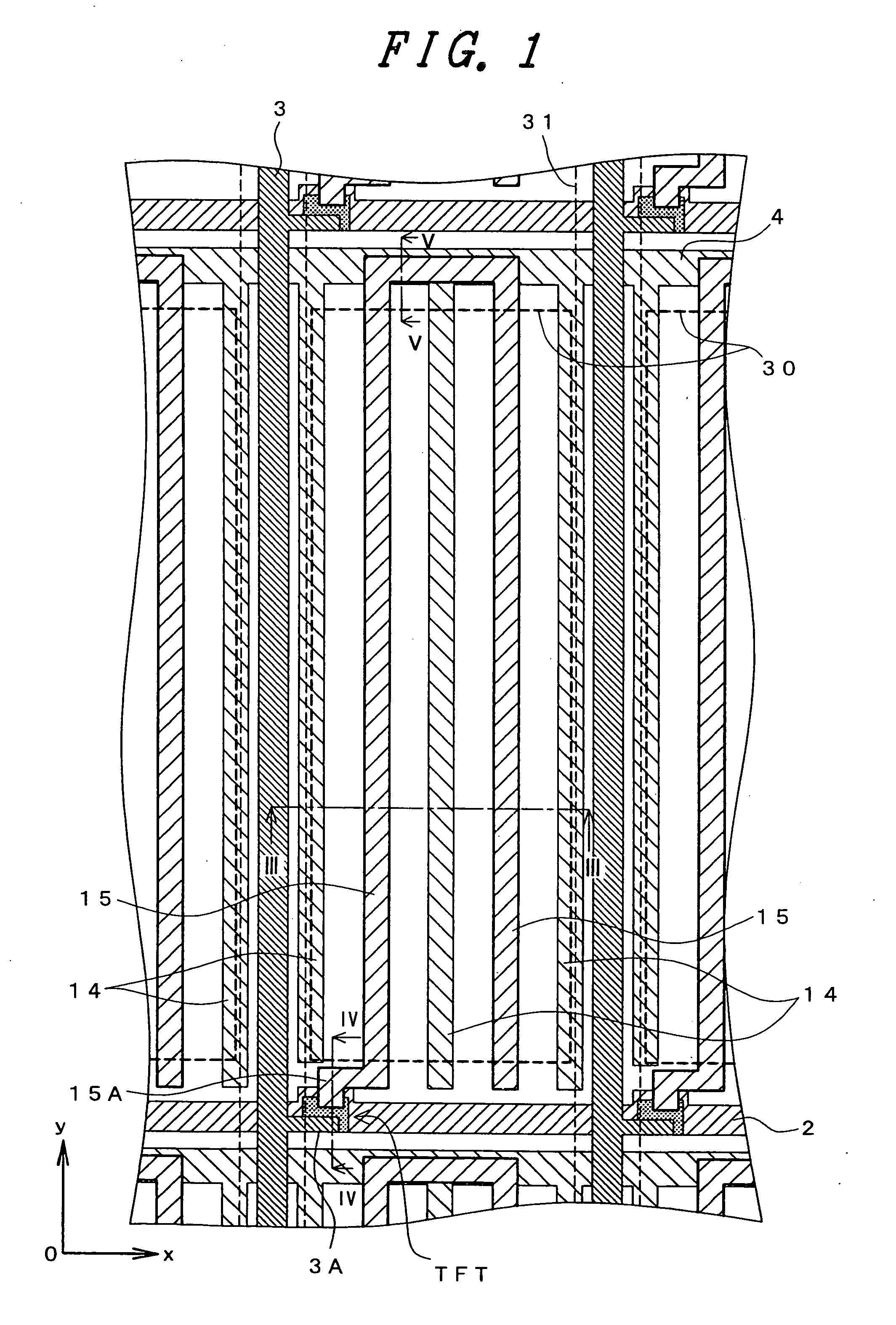
[0092] On the transparent substrate 1B on the liquid crystal layer side, a shield electrode 32 that also serves as the reference electrodes 14 are formed to overlap the video signal lines 3 extending in the y direction in the figure and adjacently arranged in the x direction. The shield electrode 32 that also serves as the reference electrodes 14 are also arranged at the center of the pixel area, extending in the Y direction. The plan view arrangement of the shield electrode 32 functioning also as the reference electrodes is s...

embodiment 3

[0102] In the third embodiment, the shield electrode 32 that also serves as the reference electrodes 14 is made of a metal such as Cr.

[0103] The disadvantage of Embodiment 2 is that because the shield electrode 32 serving also as the reference electrodes 14 is made of ITO, the part of the shield electrode 32 extending through the center of each pixel area does not block light but transmits it, deteriorating the contrast. If a light shielding layer is provided over the part of the shield electrode 32 at the center of the pixel, a deteriorated contrast can be avoided, but other problems arise including degraded aperture ratio and reduction in margin for the alignment between the upper and lower substrates.

[0104] Hence, the shield electrode 32 serving also as the reference electrodes 14 are made of a metallic material, so that the part of the shield electrode 32 at the center of the pixel has a light blocking capability and thus can improve the contrast without obviating the advantag...


PUM

PropertyMeasurementUnit
widthaaaaaaaaaa
reflectanceaaaaaaaaaa
widthaaaaaaaaaa

Abstract

An active matrix liquid crystal display device having a pair of substrates with liquid crystal layer therebetween, a plurality of video signal lines and a plurality of scan lines formed on one of the pair of substrates and a plurality of pixel electrodes connected to the video signal line through an active device and a plurality of color filters formed on another of the pair of substrates. A shield electrode which overlaps with one of the video signal lines in plane view is arranged between the one of the video signal lines and one of the color filters, and a planarization layer is arranged between one of the pixel electrodes and the shield electrode.

Description

CROSS REFERENCE TO RELATED APPLICATION [0001] This is a continuation of U.S. application Ser. No. 09 / 904,835, filed Jul. 16, 2001 and U.S. application Ser. No. 09 / 029,747, filed Mar. 2, 1998, now U.S. Pat. No. 6,266,117, which is a 371 of PCT / JP96 / 102562, filed Sep. 9, 1996, the subject matter of which is incorporated by reference herein.FIELD OF THE INVENTION [0002] The present invention relates to an active-matrix liquid crystal display device, and particularly to a liquid crystal display device of the so-called in-plane field type. BACKGROUND OF THE INVENTION [0003] In color liquid crystal display devices of the in-plane field type, one or both of two transparent substrates placed opposite to each other, with a liquid crystal layer disposed in between, have display electrodes and reference electrodes arranged in areas on the sides of the liquid crystal corresponding to unit pixels, and an electric field parallel to the transparent substrate surface is produced between the display...

Claims


Application Information

Patent Timeline
Patent Type & Authority Applications(United States)
IPC IPC(8): G02F1/1335G02F1/1343G02F1/136
CPCG02F1/133512G02F1/133707G02F1/134363G02F2201/128G02F2001/134381G02F2001/136218G02F1/1362G02F1/134381G02F1/136218G02F1/1335G02F1/1343
Inventor YANAGAWA, KAZUHIKOOHTA, MASUYUKIOGAWA, KAZUHIROASHIZAWA, KEIICHIROYANAI, MASAHIROKONISHI, NOBUTAKE
Owner PANASONIC LIQUID CRYSTAL DISPLAY CO LTD
Why Eureka
Try Eureka