Semiconductor device with buried bit line and method for fabricating the same

a technology of buried bit and fabrication method, which is applied in the direction of buried bit devices, basic electric elements, electrical appliances, etc., can solve the problems of difficult to apply such a method in terms of structural aspects, increase so as to reduce the capacitance between adjacent buried bit lines and reduce the resistance of buried bit lines. , the effect of increasing the degree of integration

Active Publication Date: 2013-09-12
SK HYNIX INC
View PDF3 Cites 15 Cited by
  • Summary
  • Abstract
  • Description
  • Claims
  • Application Information

AI Technical Summary

Benefits of technology

[0015]According to the exemplary embodiments of the present invention, since other structures (for example, a channel layer and word lines) are bonded to a substrate in which buried bit lines are formed, low resistance buried bit lines may be easily realized, and the capacitance between adjacent buried bit lines may be reduced.
[0016]Furthermore, according to the exemplary embodiments of the present invention, because a plurality of component elements constituting a vertical channel semiconductor device are separately fabricated on individual substrates and then the individual substrates are bonded with each other, structures may be simple, whereby it may be easy to increase the degree of integration, processes may be simplified, processing difficulties may be lessened, and applicability for mass production may be improved.

Problems solved by technology

However, the resistance of the buried bit line may increase due to limitations in the doping concentration of the impurity.
Although the resistance of the buried bit line may be reduced by forming the buried bit line using a metallic layer with low resistance, it may be difficult to apply such a method in terms of a structural aspect.
Nevertheless, the buried bit line with the OSC structure may have a complicated fabrication procedure, and require high difficulty fabricating technologies, and thus, it may be not easy to adapt the method for mass production.

Method used


Image

  • Semiconductor device with buried bit line and method for fabricating the same
  • Semiconductor device with buried bit line and method for fabricating the same
  • Semiconductor device with buried bit line and method for fabricating the same

Examples


first embodiment

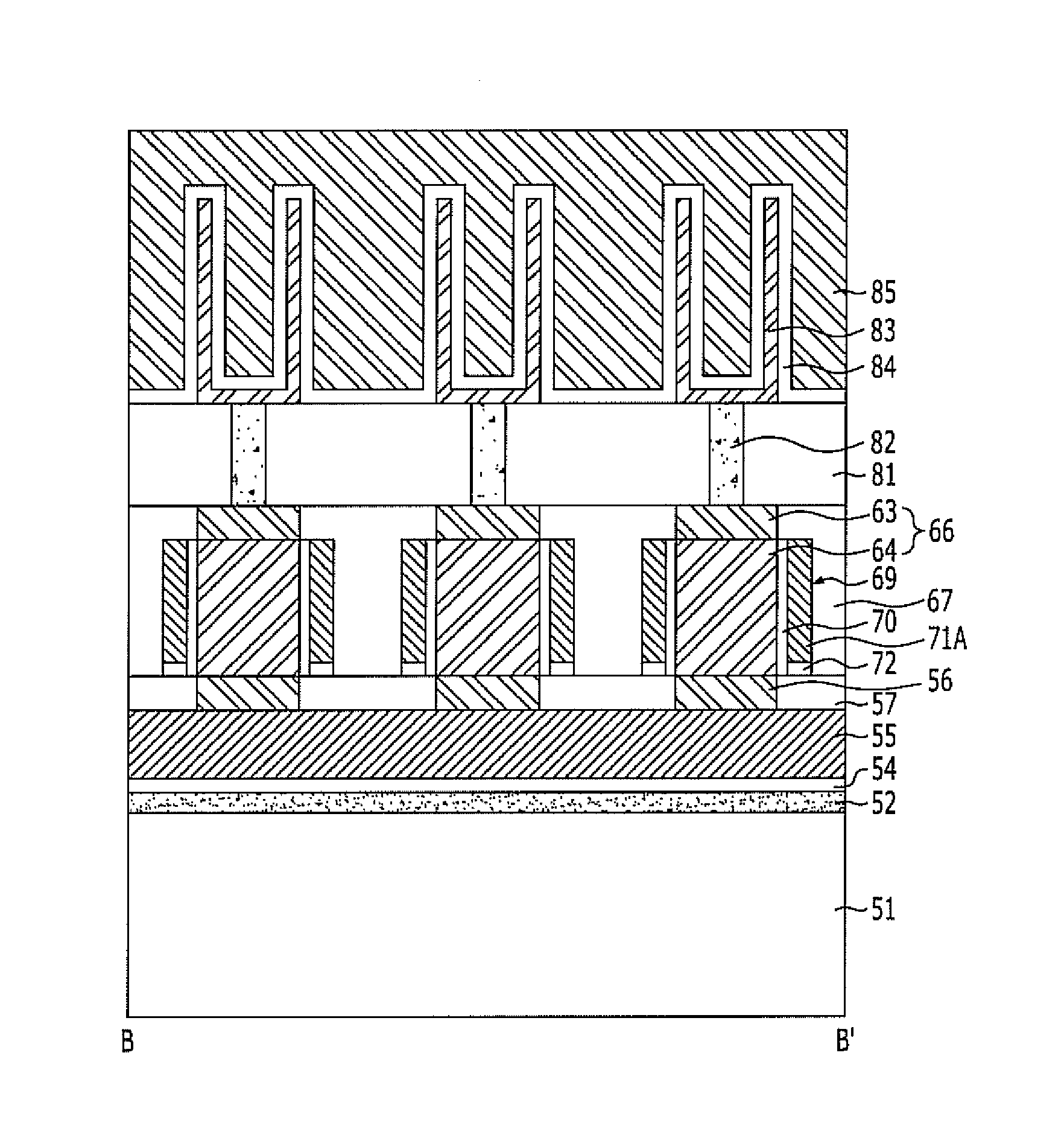
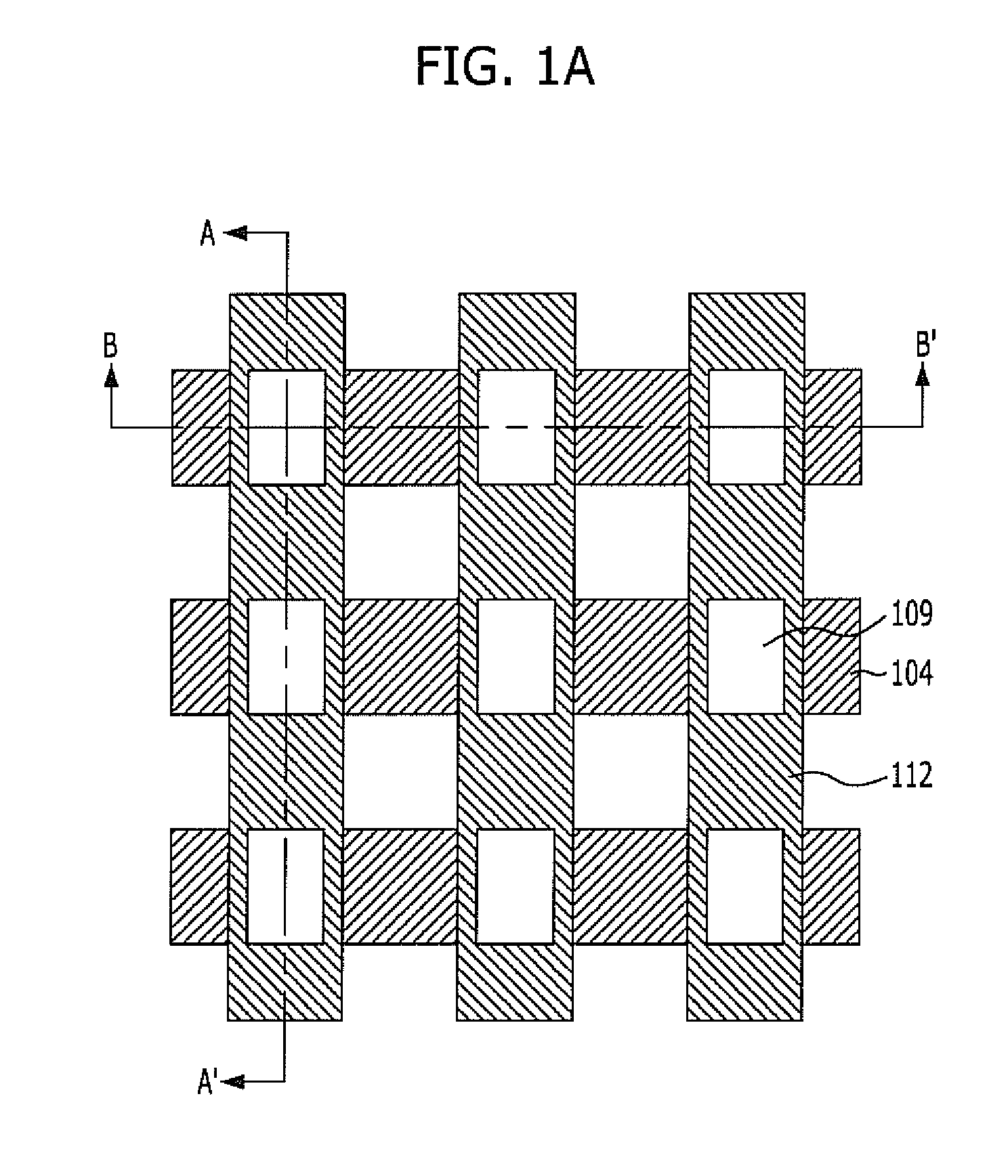
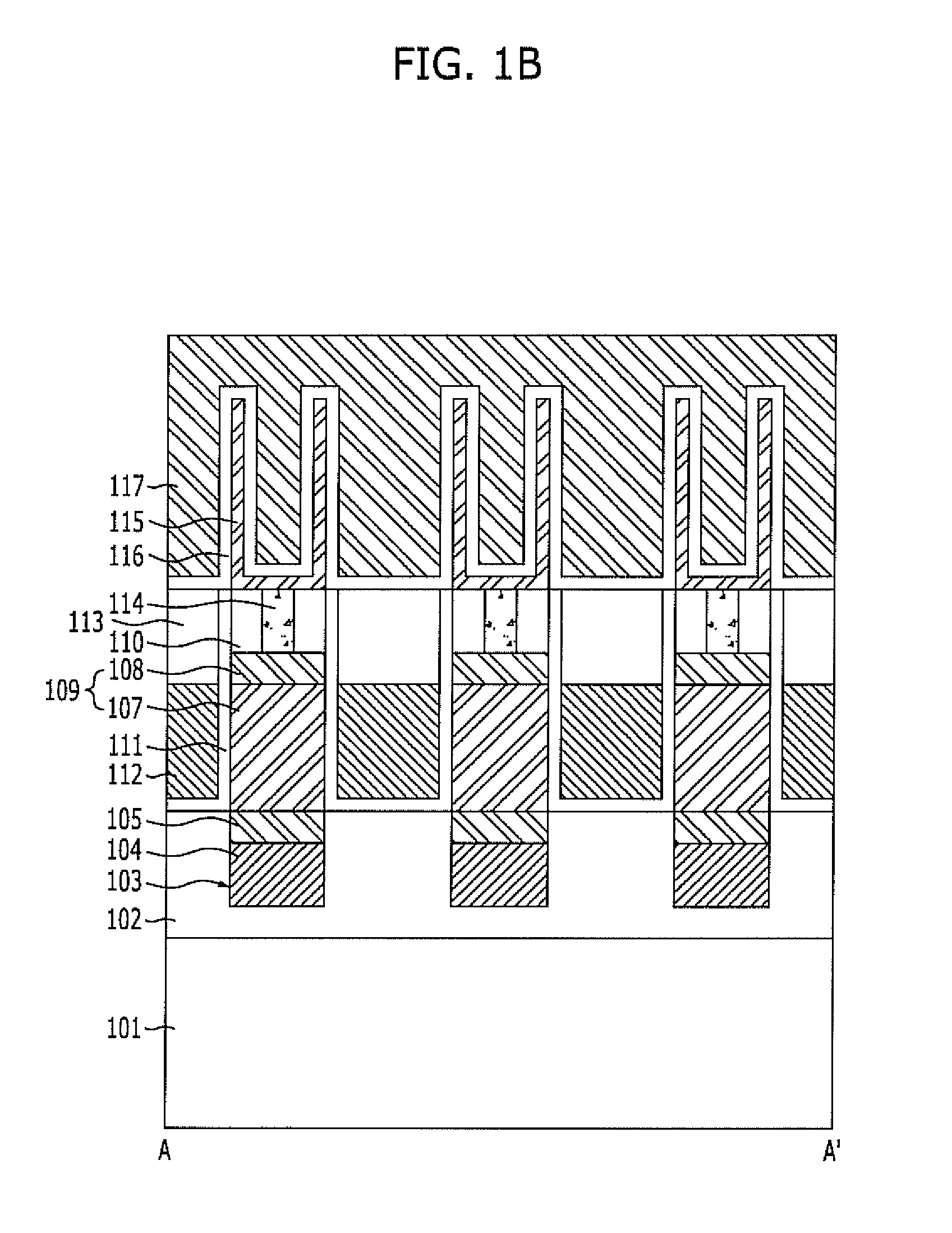
[0024]FIGS. 1A to 1C are views illustrating a semiconductor device in accordance with the present invention. FIG. 1A is a plan view, FIG. 1B is a cross-sectional view taken along the line A-A′ of FIG. 1A, and FIG. 1C is a cross-sectional view taken along the line B-B′ of FIG. 1A.

[0025]Referring to FIGS. 1A to 1C, a semiconductor device in accordance with a first embodiment of the present invention includes trenches 103 which are defined in a substrate 101, buried bit lines 104 which partially fill the trenches 103, a first source / drain layer 105 which fills the remaining portions of the trenches 103 on the buried bit lines 104, stack patterns 109 having a structure, which a channel layer 107 and a second source / drain layer 108 are stacked in, and bonded to the first source / drain layer 105 such that the channel layer 107 contacts with the first source / drain layer 105, and word lines 112 which cross with the buried bit lines 104 and are disposed adjacent to the sidewalls of the channe...

second embodiment

[0026]The trenches 103 are to provide spaces in which the buried bit lines 104 and the first source / drain layer 105 are to be formed, and the trenches 103 may be line type patterns which extend in the B-B′ direction. In order to electrically isolate adjacent buried bit lines 104 from each other and the buried bit lines 104 and the substrate 101 from each other, the trenches 103 may be defined in a first dielectric layer 102 which is formed on the substrate 101. The first dielectric layer 102 may be any one selected from the group consisting of an oxide layer, a nitride layer and an oxynitride layer. The trenches 103, in which the buried bit lines 104 and the first source / drain layer 105 are filled, may have the same shapes as first trenches according to the present invention which will be described later.

[0027]The buried bit lines 104, having shapes of partially filling the trenches 103, may include a low resistance substance, for example, a metallic layer, to improve a signal trans...


PUM


Abstract

A semiconductor device includes trenches defined in a substrate, buried bit lines partially filling the trenches, a first source / drain layer filling remaining portions of the trenches on the buried bit lines, stack patterns having a channel layer and a second source / drain layer stacked therein and bonded to the first source / drain layer, wherein the channel layer contacts with the first source / drain layer, and word lines crossing with the buried bit lines and disposed adjacent to sidewalls of the channel layer.

Description

CROSS-REFERENCE TO RELATED APPLICATIONS[0001]The present application claims priority of Korean Patent Application No. 10-2012-0024914, filed on Mar. 12, 2012, which is incorporated herein by reference in its entirety.BACKGROUND[0002]1. Field[0003]Exemplary embodiments of the present invention relate to a semiconductor device fabricating technology, and more particularly, to a semiconductor device with buried bit lines and a method for fabricating the same.[0004]2. Description of the Related Art[0005]As the degree of integration of a semiconductor memory device has increased, in order to reduce a plane area occupied by a unit cell, a cell structure has been changed from 8 F2 and 6 F2 to 4 F2 (F2: cell size factor). Various methods for forming other component elements such as transistors, bit lines, word lines, capacitors, etc. in step with such reduction in the area of the unit cell have been suggested. In particular, in order to realize a 4F2 cell structure, a vertical channel semic...

Claims


Application Information

Patent Timeline
Patent Type & Authority Applications(United States)
IPC IPC(8): H01L29/78H01L21/336
CPCH01L29/78642H01L27/10876H01L29/66666H01L27/10814H01L27/1052H01L27/10885H10B12/053H10B12/482H10B99/00H10B12/00H01L21/8238H10B12/315
Inventor HWANG, EUI-SEONG
Owner SK HYNIX INC
Why Eureka
Try Eureka