Semiconductor circuit device capable of high speed decoding

a high-speed decoding and circuit device technology, applied in electronic switching, instruments, pulse techniques, etc., can solve the problems of large load on the address signal line, delay in the change of the address signal, and longer access cycle time, so as to achieve the effect of reducing the number of operation cycles

Inactive Publication Date: 2004-10-19
RENESAS TECH CORP
View PDF4 Cites 11 Cited by
  • Summary
  • Abstract
  • Description
  • Claims
  • Application Information

AI Technical Summary

Benefits of technology

Another object of the present invention is to provide a semiconductor circuit device that can sufficiently decrease a difference in signal arrival times at decoding circuits.
A first interconnection line is connected with a plurality of logic circuits and is accompanied with the large load and the large signal propagation delay. On the other hand, a second interconnection line is not connected to a logic circuit and can transmit the signal at high speed. By electrically connecting the first and second interconnection lines at a prescribed position, a signal can be transmitted to a distal end of the first interconnection line through the second interconnection line, and accordingly, an RC delay due to a resistance and a capacitance of the first interconnection line can equivalently decrease. Thus, a variation in signal propagation delay of the first interconnection lines among the logic circuits can be decreased, and the signal can quickly be changed to perform an actual decoding operation at a faster timing.

Problems solved by technology

In regard to an address signal, as a unit decoding circuit is arranged corresponding to each memory cell row or column, a large number of decoding circuits are connected to an address signal line, which results in the large load on the address signal line.
Therefore, a line capacitance and a resistance of the address signal, or an RC time constant become greater, and thus the address signal cannot be switched at high speed, resulting in a longer access cycle time.
Particularly, when the address signal statically changes as in a static random access memory (SRAM), this delay in the change of the address signal significantly affects an operation cycle time.
Therefore, definition timings of the decoding results of the address signals are different depending on positions of the unit decoding circuits, and as an operation start timing of a subsequent circuit such as a word line drive circuit is determined based on an output signal of the unit decoding circuit of the worst case, the high-speed access cannot be achieved.
Furthermore, when the operation timing of the subsequent circuit is made as fast as possible, a margin of the subsequent circuit to the worst case circuit is reduced, and an accurate operation cannot be ensured.
In other decoding circuit which generates a signal of generating a selection signal or designating an operation mode according to a control signal as well, however, generally a large number of circuits of the same structure (repetitive circuits) are connected to a single signal line, and thus the load of the signal line becomes greater and the signal line cannot be driven at high speed.
This reference 1, however, does not consider speeding up of a decoding circuit itself which drives the word line and the disadvantage of the address signal load at all.
Although reduced resistance of a whole word line through lining (backing) by metal interconnection is described, the problem of distribution of the signal propagation delay on a single word line is not considered.
In this structure, however, regions lined and not lined by the metal interconnection exist in a single word line, and signal propagation delays distributes over one word line.
A first interconnection line is connected with a plurality of logic circuits and is accompanied with the large load and the large signal propagation delay.
Therefore, an interconnection line capacitance and an interconnection line resistance of the address signal line of the real address bus is increased, and accordingly the signal propagation delay increases.
Therefore, parasitic capacitances, as well as high resistances, are formed for first interconnection lines 20a to 20d, which causes the signal propagation delay.

Method used


Image

  • Semiconductor circuit device capable of high speed decoding
  • Semiconductor circuit device capable of high speed decoding
  • Semiconductor circuit device capable of high speed decoding

Examples


Embodiment Construction

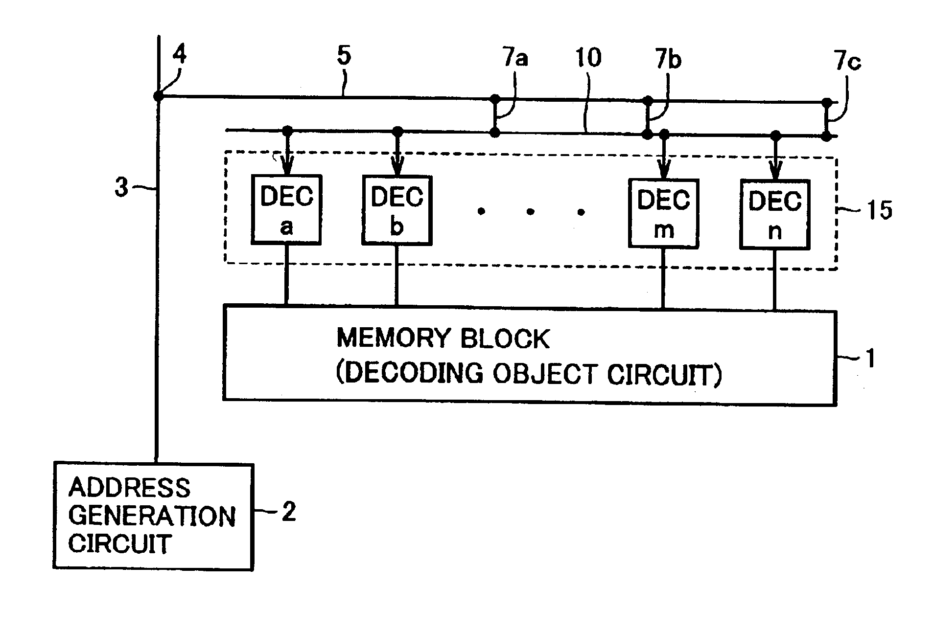
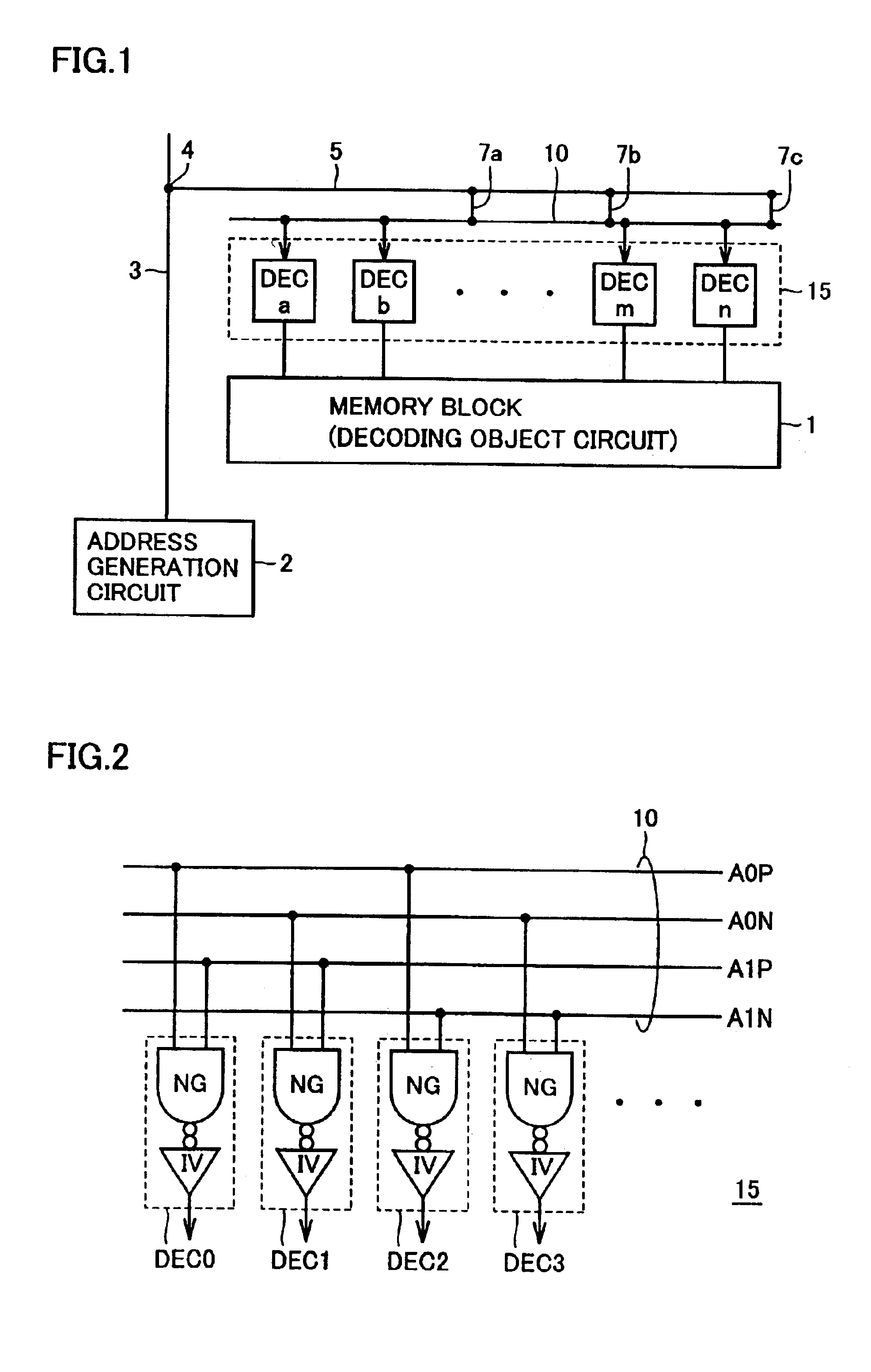
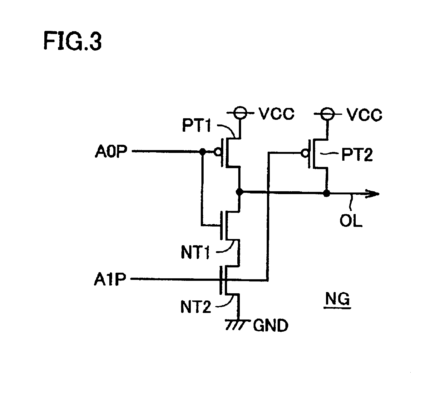
In the description above, the address decoding circuit for decoding an address signal is discussed. The present invention, however, can be applied to a configuration in which predecode signals in place of the address signal bits are transmitted and the predecode signals are further decoded.

A layout of the decoder is also not limited to the layout shown in FIG. 4, and the decoder may have another layout.

Generally, the present invention can be applied to any circuitry having the same circuit structure repeatedly arranged, decoding a received signal of a plurality of bits, and selecting an operation mode or an element according to the decoding result.

In addition, the number of address bits are not limited to four bits and, generally, the signal may be a designation signal of N bits specifying a selection object.

As described above, according to the present invention, the second interconnection lines are connected at a prescribed spacing to the first interconnection lines connecting to a...


PUM


Abstract

An address signal is transferred from an address bus transmitting an address from an address generation circuit, to a real address bus connecting to a decoder for decoding an applied address signal, via a branch node, a branch address bus and contacts. The real address bus and the branch address bus are electrically connected at a plurality of points using the contacts. The branch address bus functions as a lining or backing signal line to the real address bus, and a line resistance and line capacitance of the real address bus can be equivalently reduced. A variation in signal propagation delay over an entire decoding circuits is suppressed.

Description

1. Field of the InventionThe present invention relates to a semiconductor circuit device and, specifically, to a semiconductor circuit device for decoding a plurality of signals to generate a signal selecting a selection object element. More specifically, the present invention relates to a construction for speeding up a decoding circuit for decoding a plurality of address signals.2. Description of the Background ArtIn a semiconductor device, a circuit is widely used which selects one of a plurality of object circuits or elements according to a selection signal. A typical example of such a selection circuit is an address decoding circuit, which generates a signal for selecting data in an addressed storage location according to an address signal in a semiconductor memory device.In a SRAM (Static Random Access Memory), a DRAM (Dynamic Random Access Memory), a non-volatile memory or other memory, memory cells are arranged in rows and columns. Generally, in accessing data, a row and a co...

Claims


Application Information

Patent Timeline
Patent Type & Authority Patents(United States)
IPC IPC(8): H01L27/02G11C11/41G11C11/401G11C11/413H03K19/00
CPCH01L27/0203
Inventor KOKUBO, NOBUYUKIHOSOGANE, AKIRATOMITA, HIDEMOTO
Owner RENESAS TECH CORP
Why Eureka
Try Eureka