Photoelectric conversion element

a conversion element and photoelectric technology, applied in the direction of sustainable manufacturing/processing, climate sustainability, semiconductor devices, etc., can solve the problems of reducing the passivation effect of monocrystalline silicon substrates, reducing the characteristics of solar cells, etc., to reduce thermal strain, reduce the effect of carrier characteristics, and improve the passivation characteristics of semiconductor substrates

Inactive Publication Date: 2016-09-15
SHARP KK
View PDF1 Cites 6 Cited by
  • Summary
  • Abstract
  • Description
  • Claims
  • Application Information

AI Technical Summary

Benefits of technology

[0036]The photoelectric conversion element can be manufactured by a low-temperature process such as plasma CVD, and a decrease of carrier characteristics can be suppressed by reducing thermal strains in the n-type monocrystalline silicon substrate.
[0037]In the photoelectric conversion element according to the embodiments of the invention, the composition ratio of the desired atom is greater in the end portion on the opposite side to the semiconductor substrate side than in the en

Problems solved by technology

However, light absorption is increased by the non-crystalline silicon film, thereby posing the problem of decreasing the characterist

Method used


Image

  • Photoelectric conversion element
  • Photoelectric conversion element
  • Photoelectric conversion element

Examples


first embodiment

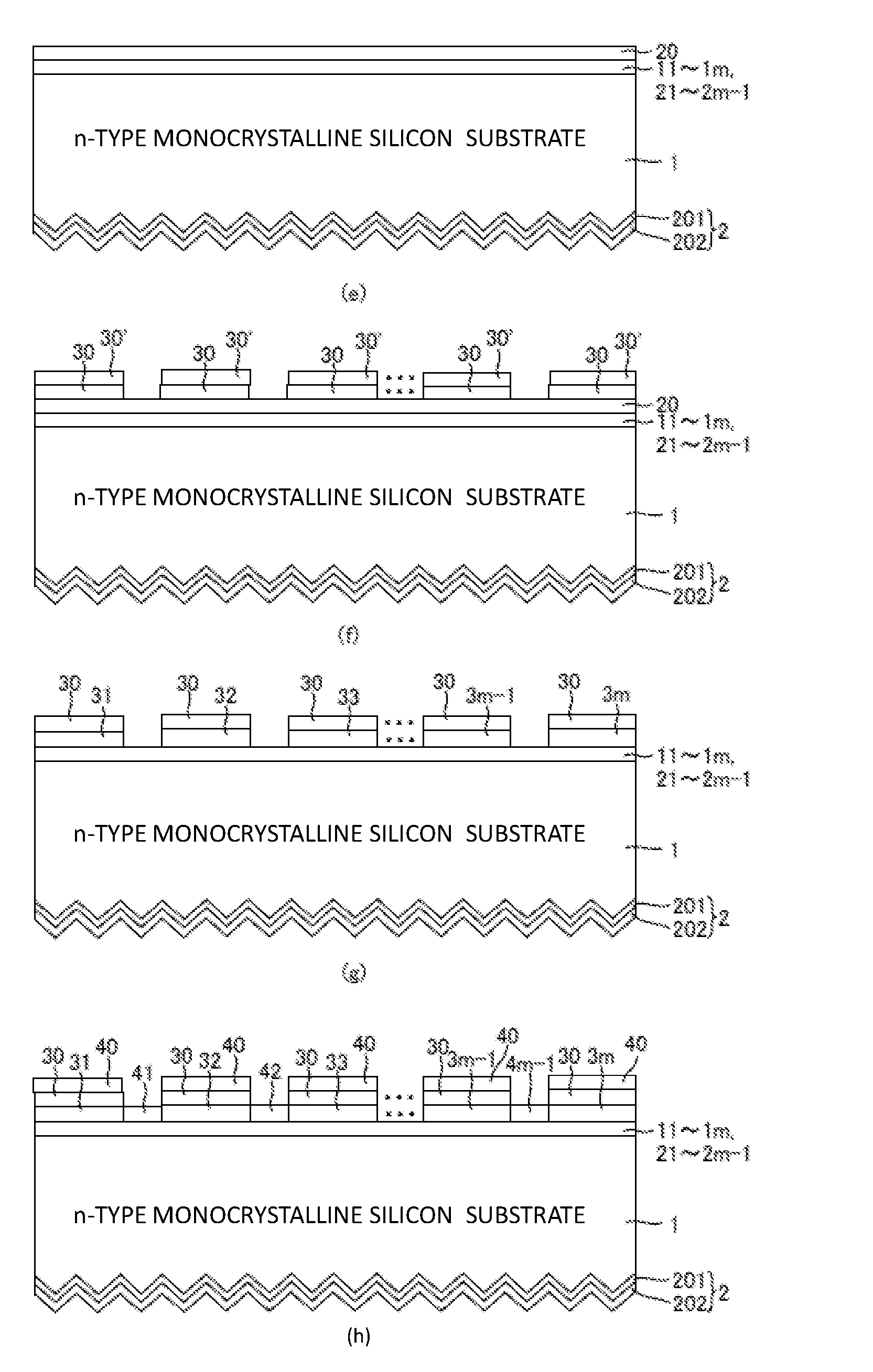
[0076]FIG. 1 is a sectional view illustrating a configuration of a photoelectric conversion element according to a first embodiment of the invention. With reference to FIG. 1, a photoelectric conversion element 100 according to the first embodiment of the invention includes an n-type monocrystalline silicon substrate 1, an non-crystalline thin film 2, i-type non-crystalline thin films 11 to 1m and 21 to 2m−1 (m is an integer greater than or equal to two), p-type non-crystalline thin films 31 to 3m, n-type non-crystalline thin films 41 to 4m−1, and electrodes 51 to 5m and 61 to 6m−1.

[0077]The n-type monocrystalline silicon substrate 1 has, for example, a (100) plane orientation and a resistivity of 0.1 Ω·cm to 1.0 Ω·cm. The n-type monocrystalline silicon substrate 1 has, for example, a thickness of 50 μm to 300 μm and preferably a thickness of 80 μm to 200 μm. The surface on the light incident side of the n-type monocrystalline silicon substrate 1 is texturized.

[0078]The non-crystall...

second embodiment

[0158]FIG. 10 is a sectional view illustrating a configuration of a photoelectric conversion element according to a second embodiment. With reference to FIG. 10, a photoelectric conversion element 200 according to the second embodiment is the same as the photoelectric conversion element 100 except that the i-type non-crystalline thin films 11 to 1m of the photoelectric conversion element 100 illustrated in FIG. 1 are removed.

[0159]In the photoelectric conversion element 200, the p-type non-crystalline thin films 31 to 3m are arranged in contact with the n-type monocrystalline silicon substrate 1.

[0160]FIG. 11 and FIG. 12 are partial process charts for manufacturing the photoelectric conversion element 200 illustrated in FIG. 10.

[0161]The photoelectric conversion element 200 is manufactured in accordance with a process in which Process (e) to Process (i) of Process (a) to Process (k) illustrated in FIG. 2 to FIG. 4 are respectively replaced by Process (e-1) to Process (i-1) illustrat...

third embodiment

[0176]FIG. 13 is a sectional view illustrating a configuration of a photoelectric conversion element according to a third embodiment. With reference to FIG. 13, a photoelectric conversion element 300 according to the third embodiment is the same as the photoelectric conversion element 100 except that the i-type non-crystalline thin films 21 to 2m−1 of the photoelectric conversion element 100 illustrated in FIG. 1 are removed.

[0177]In the photoelectric conversion element 300, the n-type non-crystalline thin films 41 to 4m−1 are arranged in contact with the n-type monocrystalline silicon substrate 1.

[0178]FIG. 14 and FIG. 15 are partial process charts for manufacturing the photoelectric conversion element 300 illustrated in FIG. 13.

[0179]The photoelectric conversion element 300 is manufactured in accordance with a process in which Process (e) to Process (i) of Process (a) to Process (k) illustrated in FIG. 2 to FIG. 4 are respectively replaced by Process (e-2) to Process (i-2) illustr...


PUM


Abstract

A photoelectric conversion element 100 includes an n-type monocrystalline silicon substrate 1, an non-crystalline thin film 2, i-type non-crystalline thin films 11 to 1m and 21 to 2m−1, p-type non-crystalline thin films 31 to 3m, and n-type non-crystalline thin films 41 to 4m−1. The non-crystalline thin film 2 is configured of non-crystalline thin films 201 and 202 and is disposed in contact with the surface on the light incident side of the n-type monocrystalline silicon substrate 1. The non-crystalline thin film 201 is configured of a-Si, and the non-crystalline thin film 202 is configured of a-SiNx (0.78≦x≦1.03). The i-type non-crystalline thin films 11 to 1m and 21 to 2m−1 are disposed in contact with the rear surface of the n-type monocrystalline silicon substrate 1. The p-type non-crystalline thin films 31 to 3m are disposed in contact with the i-type non-crystalline thin films 11 to 1m. The n-type non-crystalline thin films 41 to 4m−1 are disposed in contact with the i-type non-crystalline thin films 21 to 2m−1.

Description

TECHNICAL FIELD[0001]The present invention relates to a photoelectric conversion element.BACKGROUND ART[0002]The important things to achieve high conversion efficiency in a solar cell are suppressing reflection of light on the light-receiving surface side of the solar cell and suppressing carrier recombination on the light-receiving surface side of the solar cell. Thus, a passivation film and an antireflection coat are disposed on the light-receiving surface side of the solar cell. The antireflection coat may double as the passivation film.[0003]In PTL 1, for example, there is disclosed a heterojunction type solar cell. In the solar cell of PTL 1, intrinsic non-crystalline silicon, p-type non-crystalline silicon, and a transparent conductive film are formed on the light-receiving surface side of an n-type monocrystalline silicon substrate. In the solar cell of such a configuration, a strong interface state passivation effect is achieved in the interface between the non-crystalline s...

Claims


Application Information

Patent Timeline
IPC IPC(8): H01L31/0384H01L31/0376H01L31/028
CPCH01L31/0384H01L31/03762H01L31/028H01L31/0747H01L31/022441H01L31/1804Y02E10/547Y02E10/548Y02P70/50
Inventor KIMOTO, KENJIKOIDE, NAOKISAKAI, TOSHIHIKOKUNIYOSHI, TOKUAKI
Owner SHARP KK
Why Eureka
Try Eureka