Lattice-matched LED epitaxial structure and preparation method thereof

An epitaxial structure, lattice matching technology, applied in electrical components, circuits, semiconductor devices and other directions, can solve the problems of large lattice, band bending, can not effectively alleviate lattice strain, etc., to improve radiation recombination efficiency and internal quantum luminescence Efficiency, the effect of slowing down the decrease in luminous efficiency, and improving the quality of crystal growth

Inactive Publication Date: 2014-10-22
SHANXI FEIHONG MICRO NANO PHOTOELECTRONICS SCI & TECH
View PDF5 Cites 4 Cited by
  • Summary
  • Abstract
  • Description
  • Claims
  • Application Information

AI Technical Summary

Problems solved by technology

[0005] However, the above structure has the following disadvantages: firstly, due to the large lattice mismatch between the well layer and the barrier layer, a strong built-in electric field will be generated, which will cause the energy band to bend; secondly, due to the relatively light effective mass of electrons, There will be an overflow phenomenon; then there is a large energy level difference between the last barrier layer and the P-type electron blocking layer, which limits the injection of holes
[0006] CN103022290A provides a LED epitaxial structure with quaternary InAlGaN and its preparation method, which is characterized in that an InAlGaN stress release layer is inserted between the n-type doped GaN layer and the multi-quantum well light-emitting layer, but the thickness of this layer is 40nm -50nm, cannot effectively slow down the lattice strain between the n-type doped GaN layer and the multi-quantum well light-emitting layer
Although AlGaInN and the GaN barrier material lattice match perfectly, the lattice matching between the InGaN well material and the barrier material has not been realized, so that there is still a lattice strain between the well and the barrier.

Method used


Image

  • Lattice-matched LED epitaxial structure and preparation method thereof
  • Lattice-matched LED epitaxial structure and preparation method thereof
  • Lattice-matched LED epitaxial structure and preparation method thereof

Examples


Embodiment 1

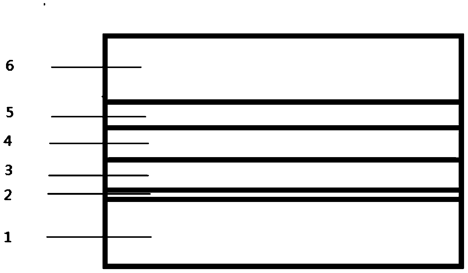
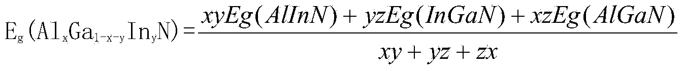
[0045] A lattice-matched LED epitaxial structure, comprising Al with a thickness of 25 nm on the substrate layer 1 0.51 Ga 0.18 In 0.31 N nucleation layer 2, undoped Al with a thickness of 1.2 μm 0.51 Ga 0.18 In 0.31 N layer 3, Si-doped Al with a thickness of 1.5 μm 0.51 Ga 0.18 In 0.31 N layer 4, multi-quantum well light-emitting layer 5 and Mg-doped Al with a thickness of 200nm 0.51 Ga 0.18 In 0.31 N layer 6; the multi-quantum well light-emitting layer 5 is 9 repeating periods and the thickness is respectively 3nm thick In 0.2 Ga 0.8 N well layer and 12nm thick Al 0.51 Ga 0.18 In 0.31 N barrier layer composition; the 1.5μm Si-doped Al 0.51 Ga 0.18 In 0.31 The N layer 4 is composed of a highly doped layer of 1.3 μm and a low doped layer of 0.2 μm, and the Si doping concentration of the high doped layer is 8×10 18 cm -3 , the Si doping concentration of the low-doped layer is 2×10 17 cm -3 .

Embodiment 2

[0047] The preparation method of the LED structure described in embodiment 1, the specific steps are as follows:

[0048] 1. Place the sapphire substrate in a hydrogen atmosphere, heat it to 1080°C and keep it for 5 minutes to remove H on the surface of the substrate 2 O and O 2 ;

[0049] 2. Under the condition of hydrogen atmosphere, adjust the temperature to heat the substrate layer to 540°C, press 500Torr, and keep it for 5 minutes. Use TMGa as the Ga source, NH3 as the N source, TMAl as the Al source, and TMIn as the In source to start growing Al 0.51 Ga 0.18 In 0.31 The N nucleation layer has a thickness of 30nm; then adjust the temperature in the MOCVD reaction chamber to 860°C and keep it for 10min to make the Al 0.51 Ga 0.18 In 0.31 The N nucleation layer undergoes recrystallization;

[0050] 3) Keep the temperature in the MOCVD reaction chamber at 860°C and the pressure at 350Torr to grow undoped Al 0.51 Ga 0.18 In 0.31 N layer 1.2μm, n-type doped Al 0.51 ...

Embodiment 3

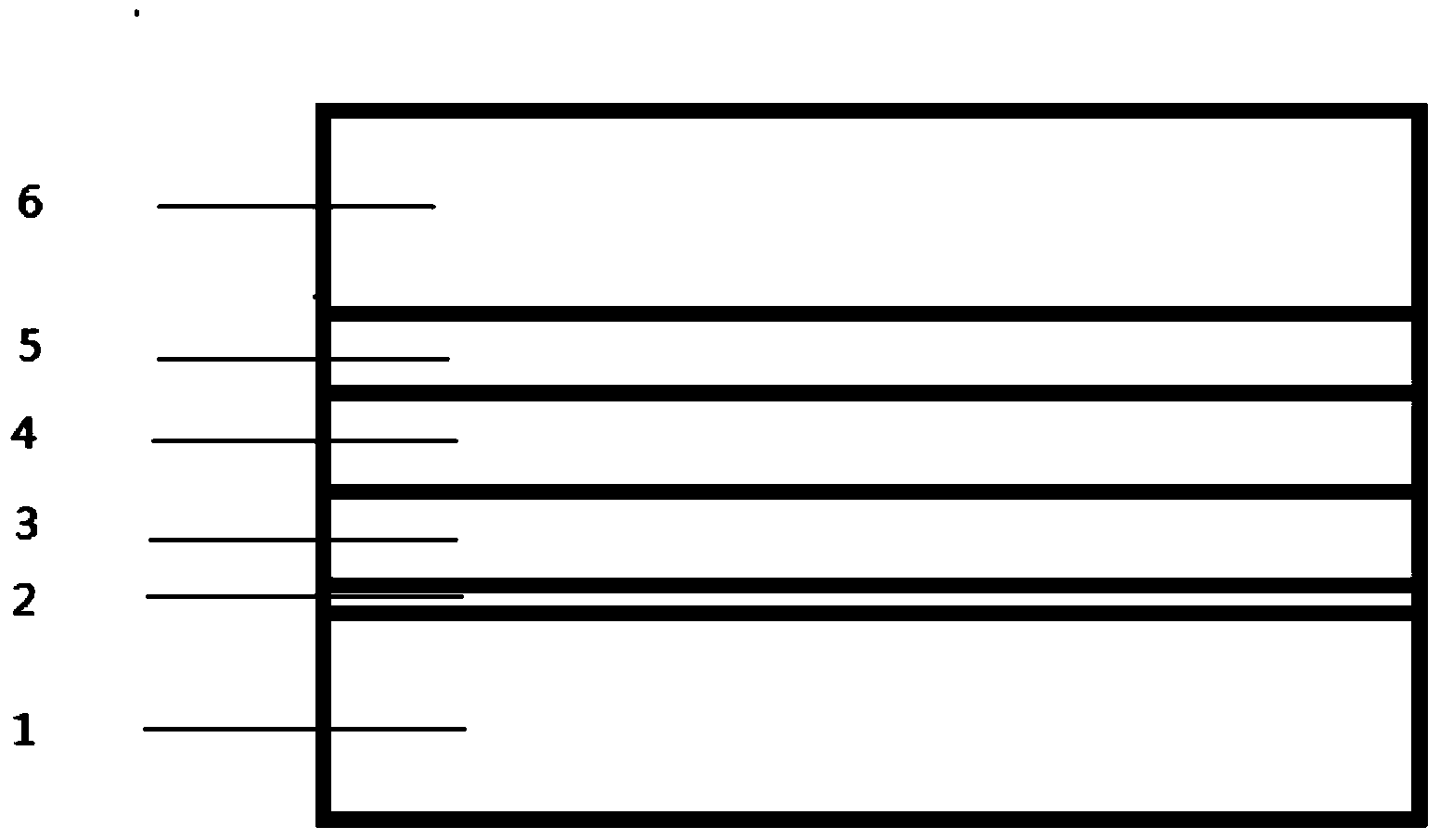
[0054] A lattice-matched LED epitaxial structure, comprising Al with a thickness of 25 nm on the substrate layer 1 0.63 Ga 0.09 In 0.28 N nucleation layer 2, undoped Al with a thickness of 1.2 μm 0.63 Ga 0.09 In 0.28 N layer 3, Si-doped Al with a thickness of 1.5 μm 0.63 Ga 0.09 In 0.28 N layer 4, multi-quantum well light-emitting layer 5 and Mg-doped Al with a thickness of 200nm 0.63 Ga 0.09 In 0.28 N layer 6; the multi-quantum well light-emitting layer 5 is 9 repeating periods and the thickness is respectively 3nm thick In 0.15 Ga 0.85 N well layer and 12nm thick Al 0.63 Ga 0.09 In 0.28 N barrier layer composition; the 1.5μm Si-doped Al 0.63 Ga 0.09 In 0.28 The N layer 4 is composed of a highly doped layer of 1.3 μm and a low doped layer of 0.2 μm, and the Si doping concentration of the high doped layer is 8×10 18 cm -3 , the Si doping concentration of the low-doped layer is 2×10 17 cm -3 .


PUM


Abstract

The invention relates to a lattice-matched LED epitaxial structure and a preparation method thereof. The invention relates to a nitride light-emitting diode epitaxial structure whose nucleating layer, undoped layer, n type layer, luminous layer and p type layer all have polarization matching and a preparation method, and belongs to the technical field of photoelectronics. The epitaxy structure is provided with a substrate, a AlxGa(1-x)-yInyN nucleating layer, an undoped AlxGa(1-x)-yInyN layer, n type doped AlxGa(1-x)-yInyN layer, a multi-quantum well luminous layer formed by a InaGa(1-a)N well layer and a AlxGa(1-x)-yInyN barrier layer, and a p type doped AlxGa(1-x)-yInyN layer in sequence from bottom to top. Compared with a traditional structure, the epitaxial structure adopts quaternary AlxGa(1-x)-yInyN material matched with luminous layer well material from the nucleating layer to a luminous layer interval and P type doped layer, thereby eliminating a piezoelectric polarization effect between well and barrier layers in the luminous layer, and improving internal quantum luminous efficiency of the LED.

Description

technical field [0001] The invention relates to a gallium nitride-based light-emitting diode, more specifically to a nitride light-emitting diode with polarization matching from a nucleation layer, an undoped layer, an n-type layer, a light-emitting layer and a p-type layer. Background technique [0002] In recent years, the LED industry has developed rapidly, and the demand for medium and high-power white LEDs is increasing. However, in order for medium and high-power white LED lighting to enter thousands of households, it is necessary to further improve the luminous brightness and luminous efficiency. [0003] The main reasons that affect the brightness of blue light are as follows: 1. It is difficult to obtain high-concentration holes; 2. The polarized electric field is relatively strong, which makes the energy band bend, causing the wave functions of electrons and holes to not completely coincide in space. , thereby reducing the radiative recombination rate of carriers,...

Claims


Application Information

Patent Timeline
Patent Type & Authority Applications(China)
IPC IPC(8): H01L33/06H01L33/32H01L33/12H01L33/00
CPCH01L33/06H01L33/007H01L33/12H01L33/325
Inventor 李天保韩蕊蕊马淑芳田海军关永莉
Owner SHANXI FEIHONG MICRO NANO PHOTOELECTRONICS SCI & TECH
Why Eureka
Try Eureka