Light-emitting diode

A technology of light-emitting diodes and light-emitting layers, applied in the direction of electrical components, circuits, semiconductor devices, etc., to achieve the effects of improving reliability and antistatic ability, improving radiation recombination efficiency, and reducing energy band tilt

Active Publication Date: 2015-01-28
QUANZHOU SANAN SEMICON TECH CO LTD
View PDF4 Cites 6 Cited by
  • Summary
  • Abstract
  • Description
  • Claims
  • Application Information

AI Technical Summary

Problems solved by technology

The structure described in this proposal has a limited range of improvement in luminous efficiency

Method used


Image

  • Light-emitting diode
  • Light-emitting diode
  • Light-emitting diode

Examples


Embodiment 1

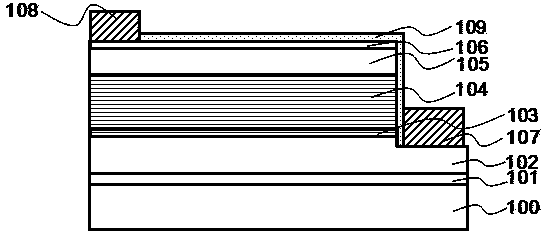
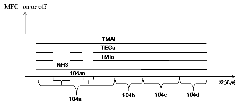
[0034] Such as figure 1 As shown, the present invention provides a multi-quantum well structure light-emitting diode with a non-uniform thickness AlN thin layer, including from bottom to top:

[0035] (1) A substrate 100, the substrate is selected from sapphire (Al 2 o 3 ), SiC, GaN or Si, and a sapphire substrate is preferred in this embodiment.

[0036] (2) A buffer layer 101 grown on the substrate 100 after high-temperature hydrogenation treatment, made of gallium nitride (GaN) and / or aluminum nitride (AlN) and / or aluminum gallium nitride (GaAlN ) layer, the growth temperature is 400~650℃, and the thickness is 1 nm~50 nm.

[0037] (3) An N-type GaN layer 102, the N-type GaN layer is grown on the buffer layer 101, the growth temperature is 1000-1200°C, the thickness is 500nm-5000nm, and the doping concentration is 1×10 18 ~1×10 20 cm -3 , preferably 1 x 10 19 cm -3 , the dopant source is preferably SiH4.

[0038] (4) A stress release layer 103 , the stress release ...

Embodiment 2

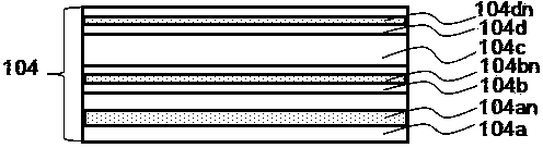
[0054] The difference from Example 1 is step (5), such as Figure 4 As shown, an AlN thin layer with non-uniform thickness is inserted in the barrier layer and the first transition layer respectively, and the thickness of the AlN thin layer in the barrier layer and the first transition layer gradually decreases along the growth direction.

Embodiment 3

[0056] The difference from Example 1 is step (5), such as Figure 5 As shown, a thin layer of AlN with a non-uniform thickness is inserted in each of the barrier layer, the first transition layer, and the second transition layer. The thickness of the AlN thin layer in the barrier layer, the first transition layer and the second transition layer decreases gradually along the growth direction.


PUM


Abstract

The invention discloses a light-emitting diode which at least comprises an N type layer, a light-emitting layer and a P type layer. The light-emitting layer is of a multi-quantum-well periodic structure and comprises a base layer, a first transition layer, a well layer and a second transition layer, wherein at least two thickness-uneven AlN thin layers are inserted among the base layer, the first transition layer and the second transition layer. The overlapping structure formed by the AlN thin layers, the base layer, the first transition layer and the second transition layer is adopted, and therefore the depolarization field of quantum well regions can be effectively modularized, the polarization charges between the well layer and the base layer are reduced, the energy band inclination is weakened, and the radiative recombination efficiency of carriers in the quantum well regions is improved.

Description

technical field [0001] The invention relates to a semiconductor device, more specifically, to a light-emitting diode with a periodic structure of multiple quantum wells of group III nitrides. Background of the invention [0002] Light-emitting diodes have the advantages of high electro-optical conversion efficiency, long service life, environmental protection, and energy saving, and have been recognized as the third-generation lighting source. GaN-based epitaxial wafer is the core component of LED and determines the performance of LED products. Luminous efficiency has become a bottleneck affecting the performance of light-emitting diodes, affecting the use of products. Therefore, reducing the polarization charge between the well barrier layers, weakening the energy band tilt, and improving the luminous efficiency of the device have become the current technical research hotspots. [0003] Chinese Patent CN201110258718 "A Method for Improving Luminous Efficiency of Light-Em...

Claims


Application Information

Patent Timeline
Patent Type & Authority Applications(China)
IPC IPC(8): H01L33/06H01L33/00
CPCH01L33/00H01L33/06
Inventor 杜伟华周启伦伍明跃李志明寻飞林郑锦坚李水清
Owner QUANZHOU SANAN SEMICON TECH CO LTD
Why Eureka
Try Eureka