Light emitting diode epitaxial wafer and manufacturing method thereof

A technology of light-emitting diodes and manufacturing methods, which is applied in the direction of electrical components, circuits, semiconductor devices, etc., can solve the problems of reducing luminous efficiency, etc., and achieve the effects of improving luminous efficiency, increasing the degree of overlap, and reducing the degree of space separation

Active Publication Date: 2019-03-29
HC SEMITEK SUZHOU
View PDF7 Cites 6 Cited by
  • Summary
  • Abstract
  • Description
  • Claims
  • Application Information

AI Technical Summary

Problems solved by technology

[0005] Since the multi-quantum well layer is composed of InGaN quantum well layers and GaN quantum barrier layers alternately arranged in multiple periods, the InGaN quantum well layers and GaN quantum barrier layers will generate stress due to lattice mismatch. As the period of the layer continues to increase, the stress between the quantum well layer and the quantum barrier layer will continue to accumulate, and the polarization effect between the InGaN quantum well layer and the GaN quantum barrier layer will become stronger and stronger, resulting in the wave function of electrons and holes Separation in spatial distribution, which reduces the luminous efficiency of the LED

Method used


Image

  • Light emitting diode epitaxial wafer and manufacturing method thereof
  • Light emitting diode epitaxial wafer and manufacturing method thereof
  • Light emitting diode epitaxial wafer and manufacturing method thereof

Examples


Embodiment Construction

[0028] In order to make the object, technical solution and advantages of the present invention clearer, the implementation manner of the present invention will be further described in detail below in conjunction with the accompanying drawings.

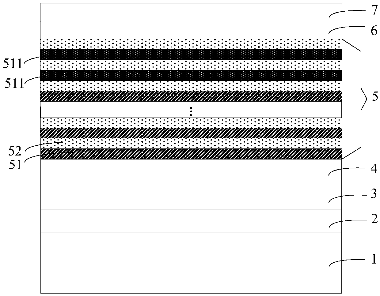
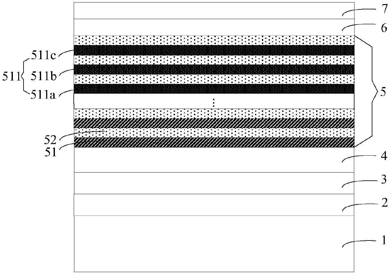
[0029] An embodiment of the present invention provides a light emitting diode epitaxial wafer, figure 1 It is a schematic structural diagram of a light-emitting diode epitaxial wafer provided by an embodiment of the present invention, as shown in figure 1 As shown, the light-emitting diode epitaxial wafer includes a substrate 1, and a low-temperature buffer layer 2, a high-temperature buffer layer 3, an N-type layer 4, a multi-quantum well layer 5, an electron blocking layer 6, and a P-type layer stacked on the substrate 1 in sequence. Layer 7, the multi-quantum well layer 5 includes a plurality of InGaN quantum well layers 51 and GaN quantum barrier layers 52 alternately grown periodically.

[0030] The plurality of InGaN quantum wel...


PUM


Abstract

The invention discloses a light emitting diode epitaxial wafer and a manufacturing method thereof and belongs to the technical field of a semiconductor. The light emitting diode epitaxial wafer includes a substrate, and a low temperature buffer layer, a high temperature buffer layer, an N type layer, a multi-quantum well layer, an electron blocking layer and a P type layer which are sequentially laminated on the substrate, wherein the multi-quantum well layer includes multiple InGaN quantum well layers and GaN quantum barrier layers which alternately grow, the multiple InGaN quantum well layers include multiple first InGaN quantum well layers adjacent to the P type layer, in the direction from the N type layer to the P type layer, thickness of the multiple first InGaN quantum well layers decreases layer by layer, the content of the In in the multiple first InGaN quantum well layers decreases layer by layer, so the polarization effect between the InGaN quantum well layers and the GaN quantum barrier layers in the multi-quantum well layer can be reduced, and thereby light emitting efficiency of LEDs is improved.

Description

technical field [0001] The invention relates to the technical field of semiconductors, in particular to a light-emitting diode epitaxial wafer and a manufacturing method thereof. Background technique [0002] LED (Light Emitting Diode, Light Emitting Diode) is a semiconductor electronic component that can emit light. As an efficient, environmentally friendly and green new solid-state lighting source, it is being rapidly and widely used, such as traffic lights, car interior and exterior lights, urban landscape lighting, mobile phone backlights, etc. [0003] The epitaxial wafer is the main component of the LED. The existing GaN-based LED epitaxial wafer includes the substrate and the low-temperature buffer layer, high-temperature buffer layer, N-type layer, multi-quantum well layer, electron blocking layer and P-type layer. The N-type layer is doped with Si to provide electrons, and the P-type layer is doped with Mg to provide holes. When the current is injected into the G...

Claims


Application Information

Patent Timeline
Patent Type & Authority Applications(China)
IPC IPC(8): H01L33/12H01L33/06H01L33/32H01L33/00
CPCH01L33/0075H01L33/06H01L33/12H01L33/32
Inventor 姚振从颖胡加辉李鹏
Owner HC SEMITEK SUZHOU
Why Eureka
Try Eureka