InGaN/GaN quantum well grown on ScMgAlO4 substrate and preparation method of InGaN/GaN quantum well

A magnesium scandium aluminate, quantum well technology, applied in electrical components, circuits, semiconductor devices and other directions, can solve the problem of unfavorable high-quality GaN thin film growth, high-performance GaN thin film device industrialization, difficult preparation of large-scale substrates, and substrates. Problems such as poor single crystal quality, to achieve the effect of being conducive to heat dissipation, releasing mismatch stress, and easy to obtain

Active Publication Date: 2016-12-07
SOUTH CHINA UNIV OF TECH
View PDF3 Cites 6 Cited by
  • Summary
  • Abstract
  • Description
  • Claims
  • Application Information

AI Technical Summary

Problems solved by technology

However, growing GaN thin films on these substrates still faces many problems
For example, although the Si substrate is cheap and large in size, the lattice mismatch between the Si substrate and the epitaxial layer is relatively large; metal substrates with high thermal conductivity are mostly face-centered cubic or body-centered cubic structures, and the grown GaN films are prone to other impurity phases; La 0.3 Sr 1.7 AlTaO 6 and LiGaO 2 There is a low lattice mismatch between the substrate and the GaN thin film, but the preparation process of the large-sized substrate is difficult, and the quality of the single crystal of the substrate is poor, which is not conducive to the growth of high-quality GaN thin film and the industrialization of high-performance GaN thin film devices

Method used


Image

  • InGaN/GaN quantum well grown on ScMgAlO4 substrate and preparation method of InGaN/GaN quantum well
  • InGaN/GaN quantum well grown on ScMgAlO4 substrate and preparation method of InGaN/GaN quantum well
  • InGaN/GaN quantum well grown on ScMgAlO4 substrate and preparation method of InGaN/GaN quantum well

Examples


Embodiment 1

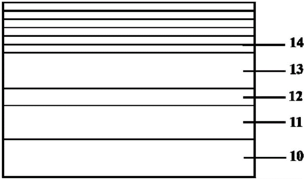
[0036] The preparation method of the InGaN / GaN multiple quantum well grown on the magnesium scandium aluminate substrate of the present embodiment comprises the following steps:

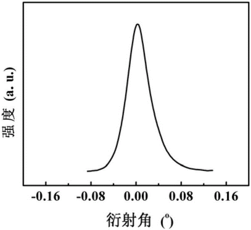
[0037] (1) Selection of the substrate and its crystal orientation: Magnesium aluminate scandium substrate is used, with the (0001) plane offset from the (11-20) plane by 0.5-1° as the epitaxial plane, and the crystal epitaxial orientation relationship is: (0001) of GaN ) plane parallel to ScMgAlO 4 (0001) face; such as figure 1 As shown, the magnesium scandium aluminate substrate used in the present invention has high crystal quality, and the XRD rocking curve half-maximum width (FWHM) value of the (0001) plane is only 20arcsec.

[0038] (2) Substrate annealing treatment, the specific process of the annealing is: the magnesium scandium aluminate substrate is annealed at 600° C. for 1 hour in the molecular beam epitaxy vacuum growth chamber of the substrate to obtain an atomically flat surface;

[003...

Embodiment 2

[0048] The preparation method of the InGaN / GaN multiple quantum well grown on the magnesium scandium aluminate substrate of the present embodiment comprises the following steps:

[0049] (1) Selection of the substrate and its crystal orientation: Magnesium aluminate scandium substrate is used, with the (0001) plane offset from the (11-20) plane by 0.5-1° as the epitaxial plane, and the crystal epitaxial orientation relationship is: (0001) of GaN ) plane parallel to ScMgAlO 4 (0001) face;

[0050] (2) Substrate annealing treatment, the specific process of the annealing is: annealing the magnesium scandium aluminate substrate at 700° C. for 2 hours in the molecular beam epitaxy vacuum growth chamber of the substrate to obtain an atomically flat surface;

[0051] (3) Epitaxial growth of the first GaN buffer layer: the substrate temperature is adjusted to 550°C, and the pressure in the reaction chamber is 4.0×10 by pulsed laser deposition technology. -5 Pa, laser energy density ...


PUM


Abstract

The invention discloses an InGaN/GaN multi-quantum well grown on a ScMgAlO4 substrate. The InGaN/GaN multi-quantum well comprises a first GaN buffer layer, an amorphous AlN insertion layer, a second GaN buffer layer and an InGaN/GaN quantum well which are sequentially grown on the ScMgAlO4 substrate. The invention also discloses a preparation method of the InGaN/GaN multi-quantum well grown on the ScMgAlO4 substrate. The InGaN/GaN multi-quantum well has the advantages of simple growth process and low preparation cost, and moreover, the prepared InGaN/GaN multi-quantum well is low in defect density, good in crystal quality and excellent in luminous performance.

Description

technical field [0001] The present invention relates to InGaN / GaN multi-quantum well and its preparation method, in particular to a kind of InGaN / GaN multiple quantum well (ScMgAlO 4 ) InGaN / GaN multiple quantum wells on a substrate and a preparation method thereof. Background technique [0002] GaN and its related group III nitrides have excellent electrical, optical, and acoustic properties, and have been widely used in the preparation of light-emitting diodes (LEDs), laser diodes (LDs), and field-effect transistors. [0003] At present, if LEDs are to be widely used on a large scale, it is necessary to further improve the luminous efficiency of LED chips. However, the luminous efficiency of commercial LEDs still needs to be improved, which is mainly due to the use of epitaxial growth on sapphire substrates. On the one hand, due to the lattice mismatch between sapphire and GaN as high as 13.3%, a high dislocation density is formed during the epitaxial GaN film process, w...

Claims


Application Information

Patent Timeline
Patent Type & Authority Applications(China)
IPC IPC(8): H01L33/06H01L33/32H01L33/02H01L33/00
CPCH01L33/0066H01L33/02H01L33/06H01L33/32
Inventor 李国强王文樑杨美娟林云昊
Owner SOUTH CHINA UNIV OF TECH
Why Eureka
Try Eureka