GaN-based nanorod LED epitaxial wafer growing on silicon/graphene composite substrate and preparation method of GaN-based nanorod LED epitaxial wafer

An LED epitaxial wafer and graphene composite technology, which is applied in nanotechnology, semiconductor/solid-state device manufacturing, electrical components, etc., can solve the problems of large tensile stress of epitaxial film, large lattice mismatch, and epitaxial film cracking, etc. Achieve the effect of reducing defect density, reducing damage and improving luminous efficiency

Inactive Publication Date: 2018-11-13
SOUTH CHINA UNIV OF TECH
View PDF4 Cites 5 Cited by
  • Summary
  • Abstract
  • Description
  • Claims
  • Application Information

AI Technical Summary

Problems solved by technology

However, the quality of GaN thin films prepared on Si substrates is not as good as that of GaN single crystal thin films prepared on sapphire substrates. A large number of dislocations appear in the GaN epitaxial layer; secondly, t

Method used


Image

  • GaN-based nanorod LED epitaxial wafer growing on silicon/graphene composite substrate and preparation method of GaN-based nanorod LED epitaxial wafer
  • GaN-based nanorod LED epitaxial wafer growing on silicon/graphene composite substrate and preparation method of GaN-based nanorod LED epitaxial wafer

Examples


Embodiment 1

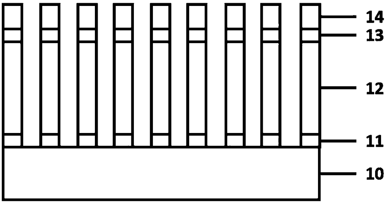
[0042] The preparation method of the GaN nanocolumn LED epitaxial wafer grown on the silicon / graphene composite substrate of the present embodiment comprises the following steps:

[0043] (1) Selection of the substrate and its crystal orientation: use a common Si substrate with a crystal orientation of (111);

[0044] (2) Substrate cleaning: Put the Si substrate into a mixed solution of HF and deionized water with a volume ratio of 1:20 and ultrasonically for 2 minutes to remove oxides and sticky dirt particles on the surface of the Si substrate, and then put it into deionized water Ultrasound for 2 minutes to remove surface impurities and blow dry with high-purity dry nitrogen;

[0045] (3) Preparation of silicon / graphene composite substrate: cut the 3-layer graphene grown on the copper foil into a size of 1 × 1 cm, soak the copper foil in a ferric chloride solution with a concentration of 1.2mol / L, The obtained graphene layer is transferred to a Si substrate, and the transf...

Embodiment 2

[0054] The preparation method of the GaN nanocolumn LED epitaxial wafer grown on the silicon / graphene composite substrate of the present embodiment comprises the following steps:

[0055] (1) Selection of the substrate and its crystal orientation: use a common Si substrate with a crystal orientation of (111);

[0056] (2) Substrate cleaning: put the Si substrate into a mixed solution of HF and deionized water with a volume ratio of 1:20 and ultrasonically for 2 minutes to remove oxides and sticky dirt particles on the surface of the silicon substrate, and then put it into deionized water Ultrasound for 1 minute to remove surface impurities and blow dry with high-purity dry nitrogen;

[0057] (3) Preparation of silicon / graphene composite substrate: Si substrate is placed in gas phase deposition equipment (CVD), carries out the growth of graphene, adopts methane as carbon source, and methane flow rate is 1 sccm, and hydrogen is carrier gas (volume The flow rate is 10cm 3 / min)...


PUM

PropertyMeasurementUnit
Heightaaaaaaaaaa
Diameteraaaaaaaaaa
Heightaaaaaaaaaa

Abstract

The invention discloses a GaN-based nanorod LED epitaxial wafer growing on a silicon/graphene composite substrate and a preparation method of the GaN-based nanorod LED epitaxial wafer. The GaN-based nanorod LED epitaxial wafer comprises non-doped GaN nanorods growing on the silicon/graphene composite substrate, n-type doped GaN layers growing on the non-doped GaN nanorods, InGaN/GaN quantum wellsgrowing on the n-type doped GaN layers and p-type doped GaN layers growing on the InGaN/GaN quantum wells. The preparation method of the GaN-based nanorod LED epitaxial wafer has the advantages of simple growth process and low preparation cost, and the prepared LED epitaxial wafer is low in defect density, good in crystallization quality and good in electrical property and optical property.

Description

technical field [0001] The invention relates to the field of LED epitaxial wafers, in particular to a GaN-based nanocolumn LED epitaxial wafer grown on a silicon / graphene composite substrate and a preparation method thereof. Background technique [0002] As a new type of solid-state lighting source and green light source, light-emitting diode (LED) has outstanding features such as energy saving, environmental protection, small size, wide range of uses and long service life. It has a wide range of applications in the fields of outdoor lighting, commercial lighting and military lighting. application. At present, under the background of the increasingly serious problem of global warming, saving energy and reducing greenhouse gas emissions have become important issues facing the world. A low-carbon economy based on low energy consumption, low pollution, and low emissions is an important direction for economic development. In the field of lighting, LED, as a new type of green s...

Claims


Application Information

Patent Timeline
IPC IPC(8): H01L33/04H01L33/06H01L33/08H01L33/20H01L33/24H01L33/32H01L33/00H01L21/02B82Y40/00
CPCH01L33/20B82Y40/00H01L21/02381H01L21/02444H01L21/02499H01L21/0254H01L21/0259H01L21/02631H01L33/007H01L33/04H01L33/06H01L33/08H01L33/24H01L33/32
Inventor 高芳亮李国强张曙光徐珍珠余粤锋
Owner SOUTH CHINA UNIV OF TECH
Why Eureka
Try Eureka