
Printed circuit board assembly

a technology of printed circuit board and assembly, which is applied in the direction of printed circuit grounding, cross-talk/noise/interference reduction, circuit electrostatic discharge protection, etc., can solve the problems of limiting the shielding from such an external inflow of static electricity, damage to an integrated circuit and an electronic component on the printed circuit board (pcb)

Active Publication Date: 2016-09-29
SAMSUNG DISPLAY CO LTD
View PDF3 Cites 24 Cited by
  • Summary
  • Abstract
  • Description
  • Claims
  • Application Information

AI Technical Summary

Benefits of technology

The present invention is about a printed circuit board that can protect against malfunctions and damage caused by electrostatic discharge (ESD). It prevents damage to the integrated circuit and electronic component on the PCB, ensuring they operate correctly.

Problems solved by technology

In this case, a malfunction of, and damage to, an integrated circuit and an electronic component on a printed circuit board (PCB) may occur due to externally generated electrostatic discharge (ESD).
Leakage current, and the like, generated by ESD may result in a hard-error that causes a physical defect (e.g., damage to an element or a component) of an integrated circuit and an electronic component on a PCB, and / or a soft-error that causes a malfunction of a device.
However, there is a limit in shielding from such an external inflow of static electricity through a bonding portion at which ground wirings are bonded to one another.

Method used


Image

  • Printed circuit board assembly
  • Printed circuit board assembly
  • Printed circuit board assembly

Examples


Embodiment Construction

[0044]Hereinafter, example embodiments of the present invention will now be described in more detail with reference to the accompanying drawings.

[0045]However, the present invention may be embodied in various different forms, and should not be construed as being limited to the exemplary embodiments set forth herein. Rather, these exemplary embodiments are provided so that this disclosure will be thorough and complete, and will fully convey the spirit and scope of the present invention to those skilled in the art.

[0046]In the drawings, the relative sizes of elements, layers, and regions may be exaggerated for clarity. Spatially relative terms, such as “beneath,”“below,”“lower,”“under,”“above,”“upper,” and the like, may be used herein for ease of explanation to describe one element's or feature's relationship to another element(s) or feature(s) as illustrated in the figures. It will be understood that the spatially relative terms are intended to encompass different orientations of the...


PUM


Abstract

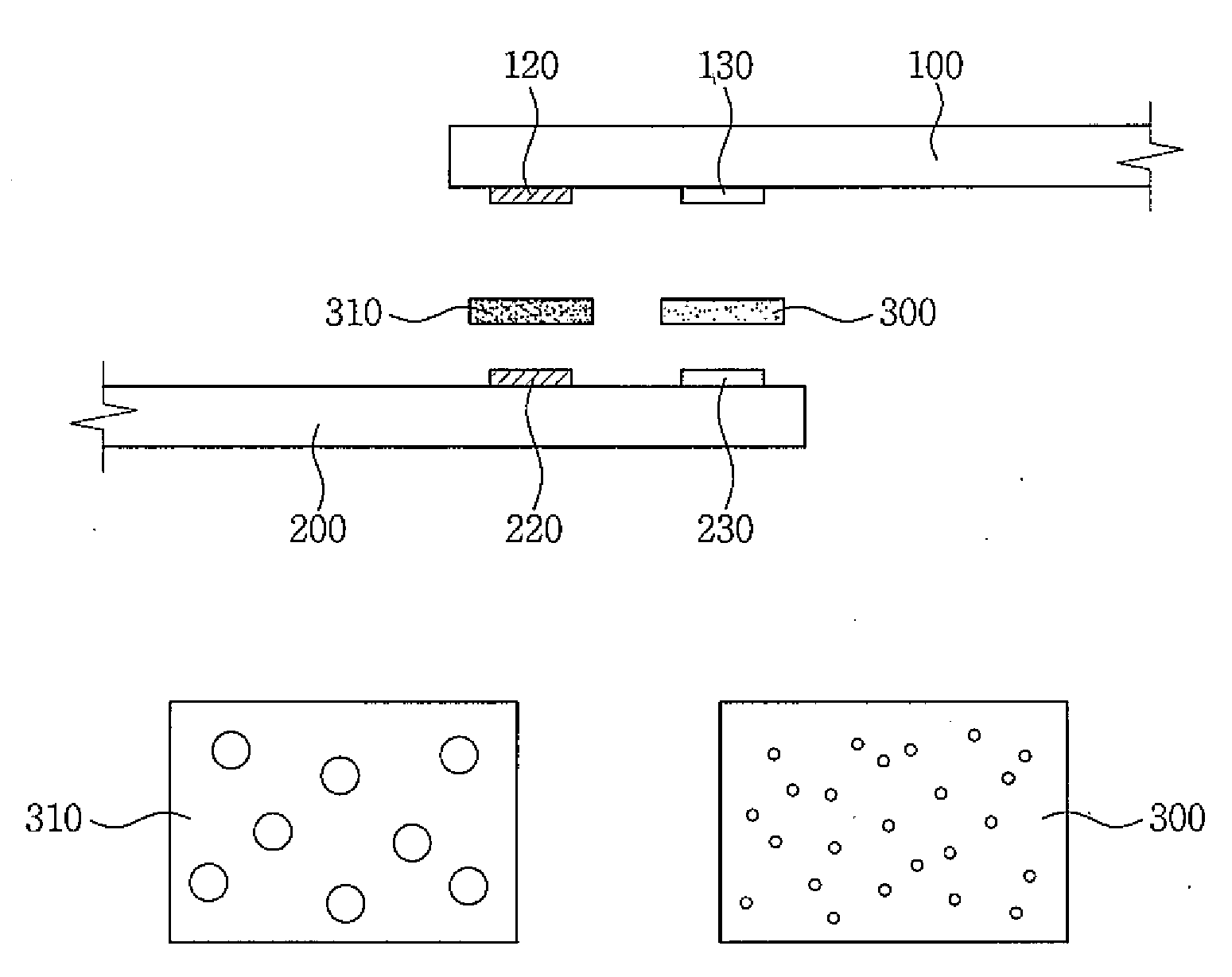
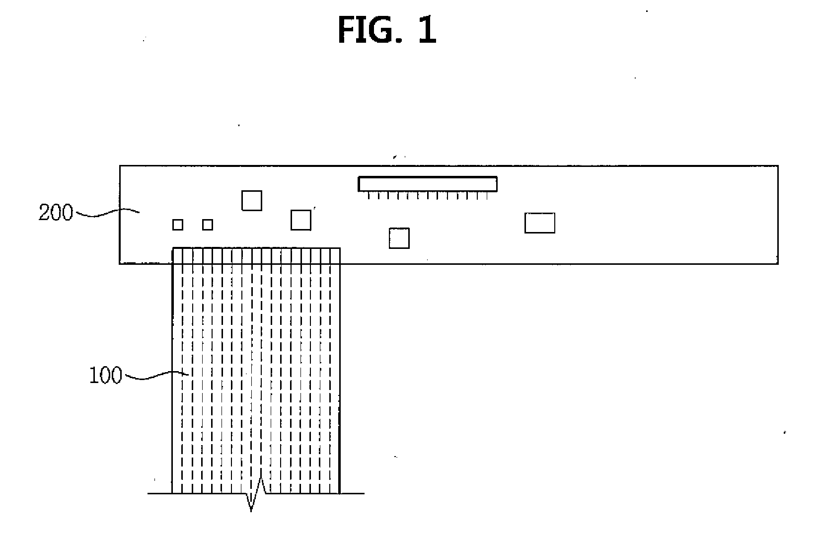
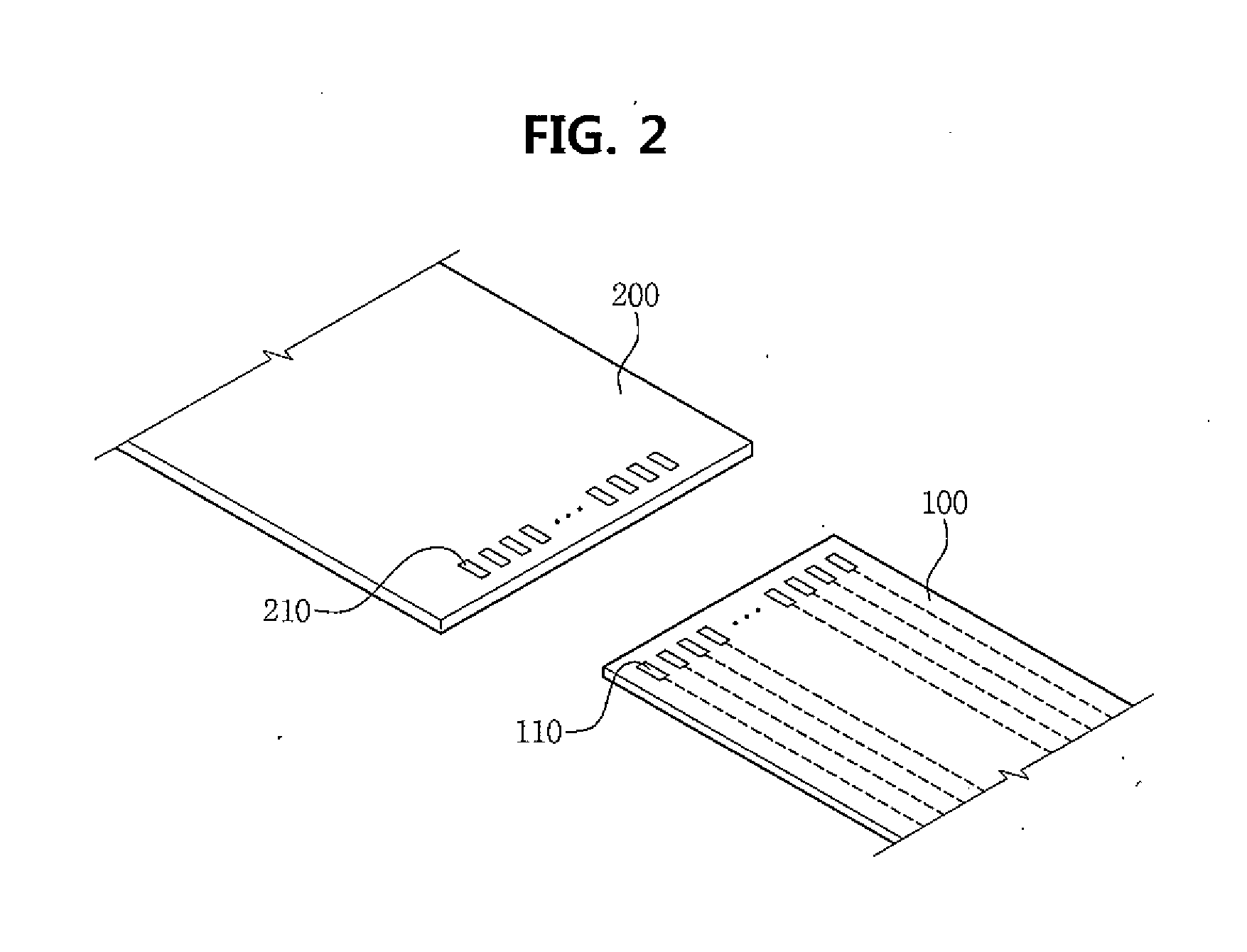
A printed circuit board assembly includes: a first signal terminal row including a plurality of first signal terminals connected to a plurality of signal wirings of a flexible printed circuit board (FPCB), respectively; a first ground terminal row spaced from the first signal terminal row and including a plurality of first ground terminals connected to a plurality of ground wirings of the FPCB, respectively; a second signal terminal row including a plurality of second signal terminals connected to a plurality of signal wirings of a printed circuit board (PCB), respectively; and a second ground terminal row spaced from the second signal terminal row and including a plurality of second ground terminals connected to a plurality of ground wirings of the PCB, respectively. The first ground terminal row is closer to an end portion of the FPCB than the first signal terminal row.

Description

CROSS-REFERENCE TO RELATED APPLICATION[0001]This application claims the priority to and all the benefits accruing under 35 U.S.C. §119 of Korean Patent Application No. 10-2015-0040184, filed on Mar. 23, 2015, with the Korean Intellectual Property Office (KIPO), the disclosure of which is incorporated herein in its entirety by reference.BACKGROUND[0002]1. Field[0003]One or more aspects of example embodiments of the present invention relate to an organic light emitting diode (“OLED”) display device.[0004]2. Description of the Related Art[0005]Display devices, such as televisions (TVs) or monitors that output image information, include image display devices that display images, and circuit devices that output image signals for displaying the images. With the development of information technology in society, demands for display devices have been diversified, thus leading to an increased use of large size flat panel display (“FPD”) devices, such as liquid crystal display (“LCD”) devices ...

Claims


Application Information

Patent Timeline
IPC IPC(8): H05K1/14
CPCH05K1/147H05K2201/09409H05K2201/09427H05K2201/041H05K1/0259H05K3/323H05K3/361H05K2201/10128H05K1/0215
Inventor CHOI, DONGWAN
Owner SAMSUNG DISPLAY CO LTD
Learn More