Plasma Generation and Control Using a DC Ring

US20160300738A1Active Publication Date: 2016-10-13TOKYO ELECTRON LTD
9 Cites 9 Cited by

Patent Information

Authority / Receiving Office
US · United States
Current Assignee / Owner
Publication Date
2016-10-13

Smart Images

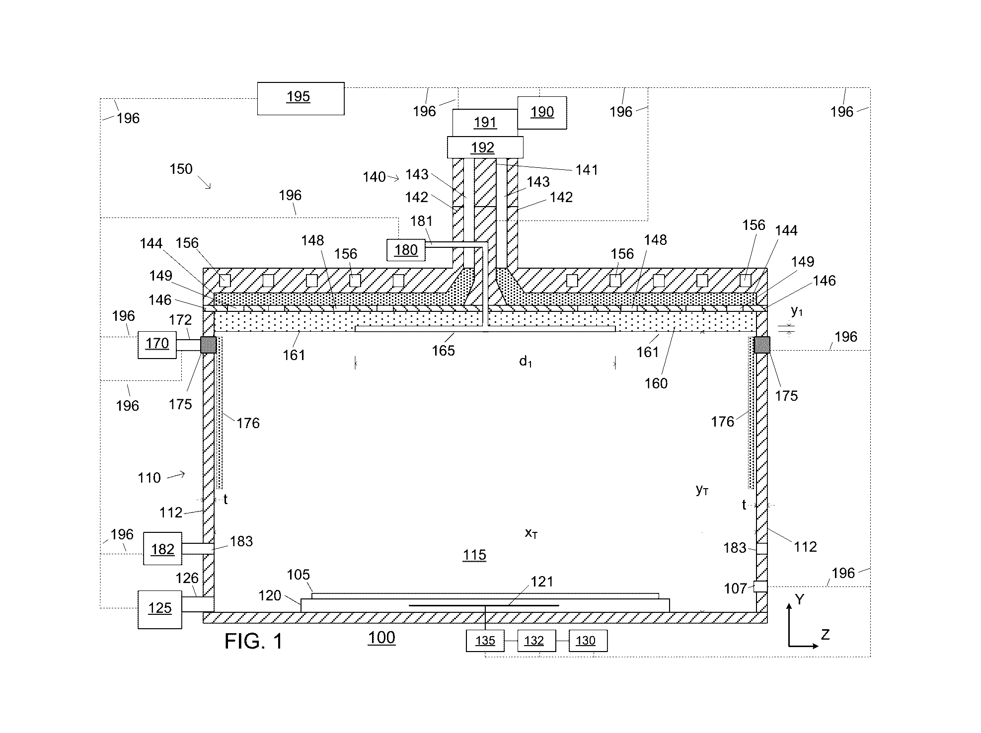
  • Figure 1
    Figure 1
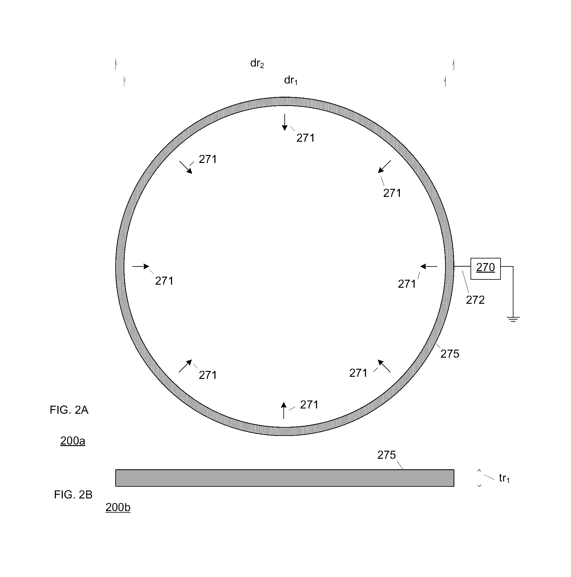
  • Figure 2
    Figure 2
  • Figure 3
    Figure 3
Patent Text Reader

Abstract

The present invention provides a SWP (surface wave plasma) processing system that does not create underdense conditions when operating at low microwave power and high gas pressure, thereby achieving a larger process window. The DC ring subsystem can be used to adjust the edge to central plasma density ratio to achieve uniformity control in the SWP processing system.
Need to check novelty before this filing date? Find Prior Art

Description

[0001] This application is based on and claims the benefit of and priority to copending U.S. Provisional Patent Application No. 62 / 144,128, entitled “Plasma Generation and Control using a DC Ring”, filed on Apr. 7, 2015, the entire contents of which are herein incorporated by reference.BACKGROUND OF THE INVENTION

[0002] 1. Field of the Invention

[0003] The present invention relates to substrate / wafer processing, and more particularly to Surface Wave Plasma (SWP) processing systems and methods for processing substrates and / or semiconductor wafers using SWP processing systems.

[0004] 2. Description of the Related Art

[0005] Typically, during semiconductor processing, a (dry) plasma etch process is utilized to remove or etch material along fine lines or within vias or contacts patterned on a semiconductor substrate. The plasma etch process generally involves positioning a semiconductor substrate with an overlying patterned, protective layer, for example a photoresist layer, into a process chamb...

Examples

Embodiment Construction

[0029]SWP plasma sources and SWP processing systems are disclosed in various embodiments. However, one skilled in the relevant art will recognize that the various embodiments may be practiced without one or more of the specific details, or with other replacement and / or additional methods, materials, or components. In other instances, well-known structures, materials, or operations are not shown or described in detail to avoid obscuring aspects of various embodiments of the invention.

[0030]Similarly, for purposes of explanation, specific numbers, materials, and configurations are set forth in order to provide a thorough understanding of the invention. Nevertheless, the invention may be practiced without specific details. Furthermore, it is understood that the various embodiments shown in the figures are illustrative representations and are not necessarily drawn to scale.

[0031]Reference throughout this specification to “one embodiment” or “an embodiment” or variation thereof means tha...