Method for fabricating a trench power MOSFET

a technology of trench power mosfet and trench power mosfet, which is applied in the direction of semiconductor devices, basic electric elements, electrical apparatus, etc., can solve the problems of deviation of defined patterns, cd of the critical dimension of the device becomes smaller, and the gate electric resistance increases, so as to improve the on-off response rate of the device, reduce the contact resistance and the connection resistance (rdson) the effect of reducing the gate resistan

Inactive Publication Date: 2006-08-01
EPISIL TECH INC
View PDF2 Cites 4 Cited by
  • Summary
  • Abstract
  • Description
  • Claims
  • Application Information

AI Technical Summary

Benefits of technology

[0018]As mentioned previously, the present invention relates to a method of fabricating the trench power MOSFET (Metal Oxide Semiconductor Field Effect Transistor), through which the problems of asymmetric source region is avoided and the on-off response rate for the transistors is improved.
[0031]In conclusion, the gate layer of the present invention replaces the conventional patterned photoresist layer as a mask for ion implantation to form the source region. Therefore, the present invention can prevent the prior problems by using the patterned photoresist layer. Beside, there is no asymmetric problem for the source region by using the spacer as a mask for the etching process.
[0032]In addition, while defining the contact opening, the spacer can effectively protect the source region and allows a bigger process window for the etching process, so that the self-aligned contact opening is formed. Besides, the metal silicide layer is formed on the surfaces of the gate layer and the exposed opening can reduce the gate electric resistance and improve the on-off response rate of the devices. At the same time, the contact resistance and the connect resistance (Rdson) are both reduced, and the reliability of the device is improved.

Problems solved by technology

However, for the planar gate, the design of minimal gate length may hinder the increase of the device intensity.
However, following demands for higher integration, the critical dimension (CD) of the device becomes smaller.
The previously mentioned patterned photoresist layer 114 may collapse or peel due to its small size, which further leads to deviation of the defined pattern.
Besides, during the formation of the source region 116, the patterned photoresist layer 114 can easily be damaged by high current implantor during the ion implementation process, which can cause errors for definition.
Furthermore, during the formation of the contact window opening 120 (as shown in the FIG. 1H), misalignment is likely to happen, which causes abnormal electrical connection and reduce the reliability of devices.

Method used


Image

  • Method for fabricating a trench power MOSFET
  • Method for fabricating a trench power MOSFET
  • Method for fabricating a trench power MOSFET

Examples


Embodiment Construction

[0035]Reference will now be made in detail to the present preferred embodiments of the invention, examples of which are illustrated in the accompanying drawings. Wherever possible, the same reference numbers are used in the drawings and the description to refer to the same or like parts.

[0036]The embodiment of the present invention is explained by an n-type doping substrate, an n-type epitaxial layer, a p-type body well region and an n-type power MOSFET. However, the modification and adoption can be made for the practical application, and the embodiment is not used to limit the present invention.

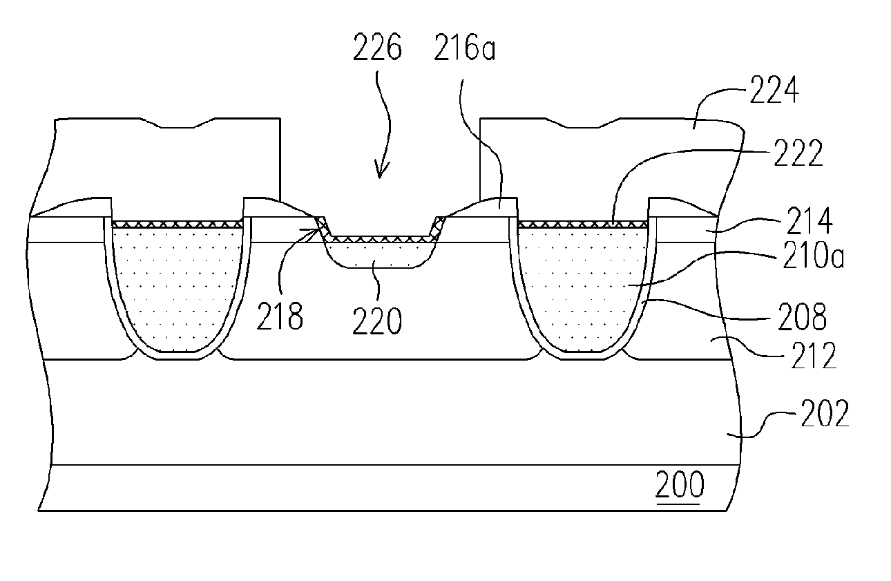
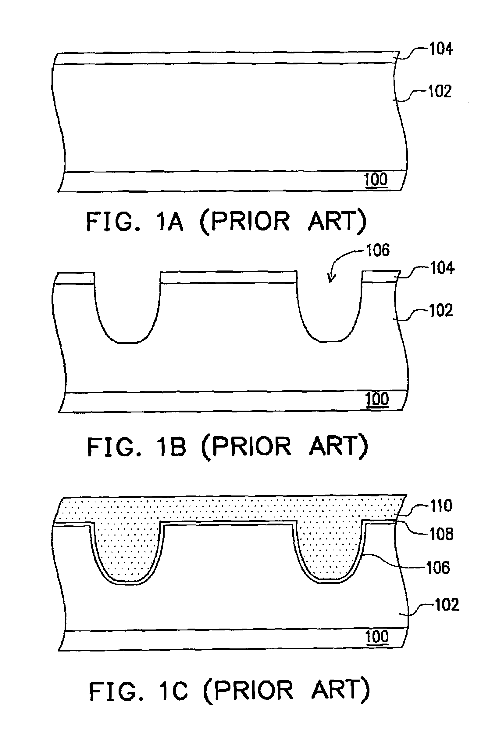
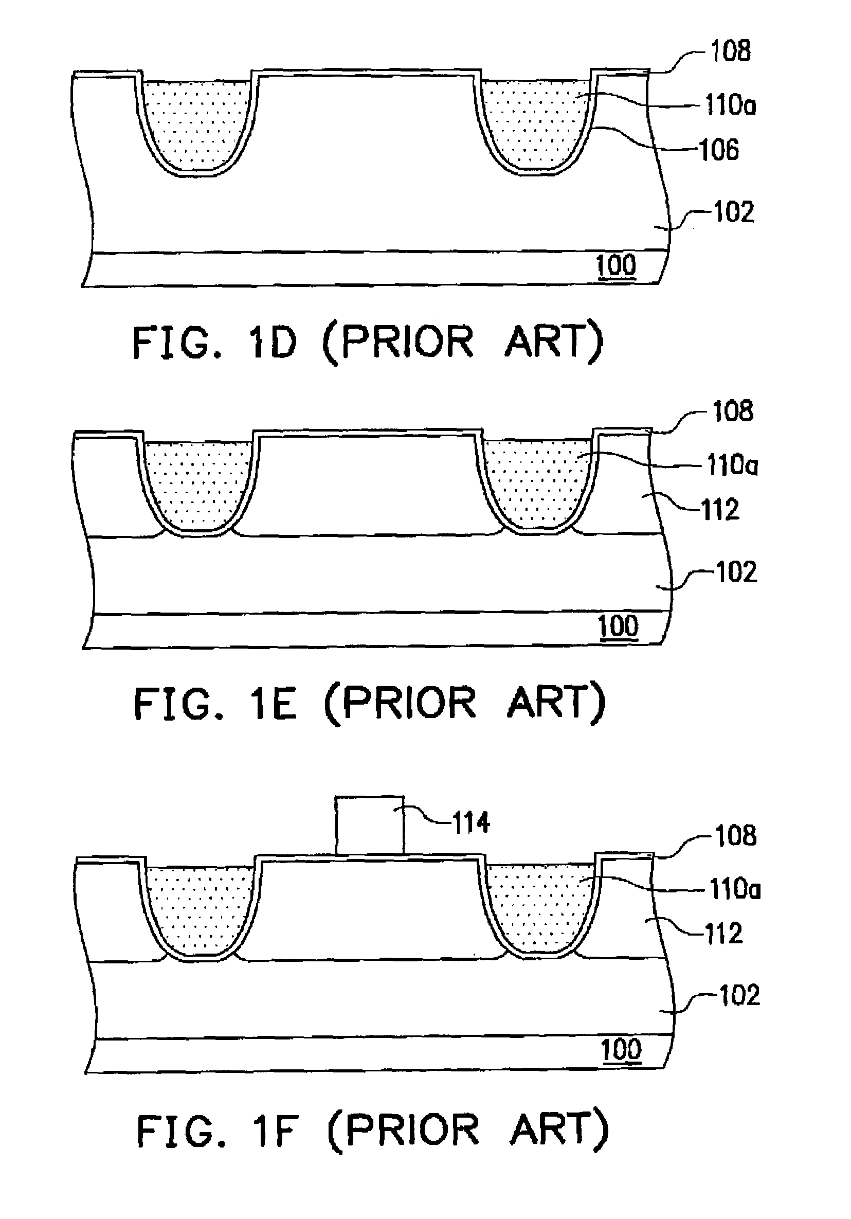
[0037]FIGS. 2A to 2J are cross sectional view of the fabrication process for the trench power MOSFET, according to the preferred embodiment of the present invention.

[0038]First, referring to FIG. 2A, a substrate 202 with an epitaxial layer 202 is provided, and the material for the epitaxial layer 202 can be, for example, an n-type doping silicon with a lower doping concentration than the con...


PUM


Abstract

A method for fabricating a trench power MOSFET, comprising an epitaxial layer and a mask layer formed over a substrate, a trench formed in the epitaxial layer and the mask layer, a gate oxide layer formed on the trench, then the mask layer removed, a body well region formed in the epitaxial layer beside the trench, a source region formed in and adjacent to the body well region, and a spacer formed on the sidewalls of the exposed gate layer exposing the source region partially. Masking by spacer, an opening exposing the body well is formed by partially removing the source region and the gate layer. A body region is formed in the body well region under the opening. A silicide layer is formed on the surfaces of the gate layer and the opening.

Description

BACKGROUND OF THE INVENTION[0001]1. Field of the Invention[0002]The present invention relates to a power MOSFET (Metal Oxide Semiconductor Field Effect Transistor), and more particularly, to a trench power MOSFET (Metal Oxide Semiconductor Field Effect Transistor) and method for fabricating the power MOSFET.[0003]2. Description of Related Art[0004]A power MOSFET can be applied to be a high voltage device with the operation voltage up to over 4,500 volts. The methods for fabricating the conventional power device are similar to the general methods used for semiconductor fabrication, and its gate is formed on the surface of the silicon substrate, i.e. a planar gate. However, for the planar gate, the design of minimal gate length may hinder the increase of the device intensity. Therefore, the trench gate structure, which may greatly reduce the device size, has become the trend in power device fabrication.[0005]FIGS. 1A–1I are the cross sectional views for the fabrication processes of th...

Claims


Application Information

Patent Timeline
Patent Type & Authority Patents(United States)
IPC IPC(8): H01L21/336H01L21/76H01L29/45H01L29/49
CPCH01L29/66734H01L29/66727H01L29/66719H01L29/456H01L29/4933
Inventor HSU, HSIU-WEN
Owner EPISIL TECH INC
Why Eureka
Try Eureka