Fabrication method of flash memory

a technology of flash memory and fabrication method, which is applied in the direction of semiconductor devices, electrical equipment, basic electric elements, etc., can solve the problems of inability to meet the requirements of high integration and uniform electrical properties of conventional flash memory structures, inability to meet the requirements of size reduction and suitable process window for lithography process, and inability to reduce the size of the gate structure. , to achieve the effect of reducing the contact resistance between the fourth conductive layer and the metallic conductive plug, the gate structur

Inactive Publication Date: 2007-02-08
POWERCHIP SEMICON CORP
View PDF5 Cites 3 Cited by
  • Summary
  • Abstract
  • Description
  • Claims
  • Application Information

AI Technical Summary

Benefits of technology

[0029] With the fabrication method provided by the present invention, no inter gate dielectric layer is formed in the gate structure in the peripheral circuitry region, and the fourth conductive layer is electrically connected to the second conductive layer in the gate structure. Accordingly, one lithography and etching process is performed to the gate structure using the fourth conductive layer as the etch-stop layer to form the conductive plug and the conductive plug can electrically connect the gate structure to the external. With only one lithography and etching process is performed for the gate structure, a larger process window is provide and the size of the gate structure may be smaller. Moreover, since the material of the fourth conductive layer is polycide, the contact resistance between the fourth conductive layer and the metallic conductive plug can be reduced dramatically. On the other hand, since the third conductive layer is protective to the inter gate dielectric layer, the above-mentioned step of removing the patterned photoresist layer will not damage the inter gate dielectric layer in the memory cell region.

Problems solved by technology

Therefore, the conventional flash memory structure cannot meet the requirements of high integration and uniform electrical properties.
For the flash memory as illustrated in FIG. 1B, it is difficult to satisfy the requirement of size reduction and suitable process window for the lithography process.
Hence, the size of the gate structure can not be reduced and the integration of the memory may not be increased.

Method used


Image

  • Fabrication method of flash memory
  • Fabrication method of flash memory
  • Fabrication method of flash memory

Examples


Embodiment Construction

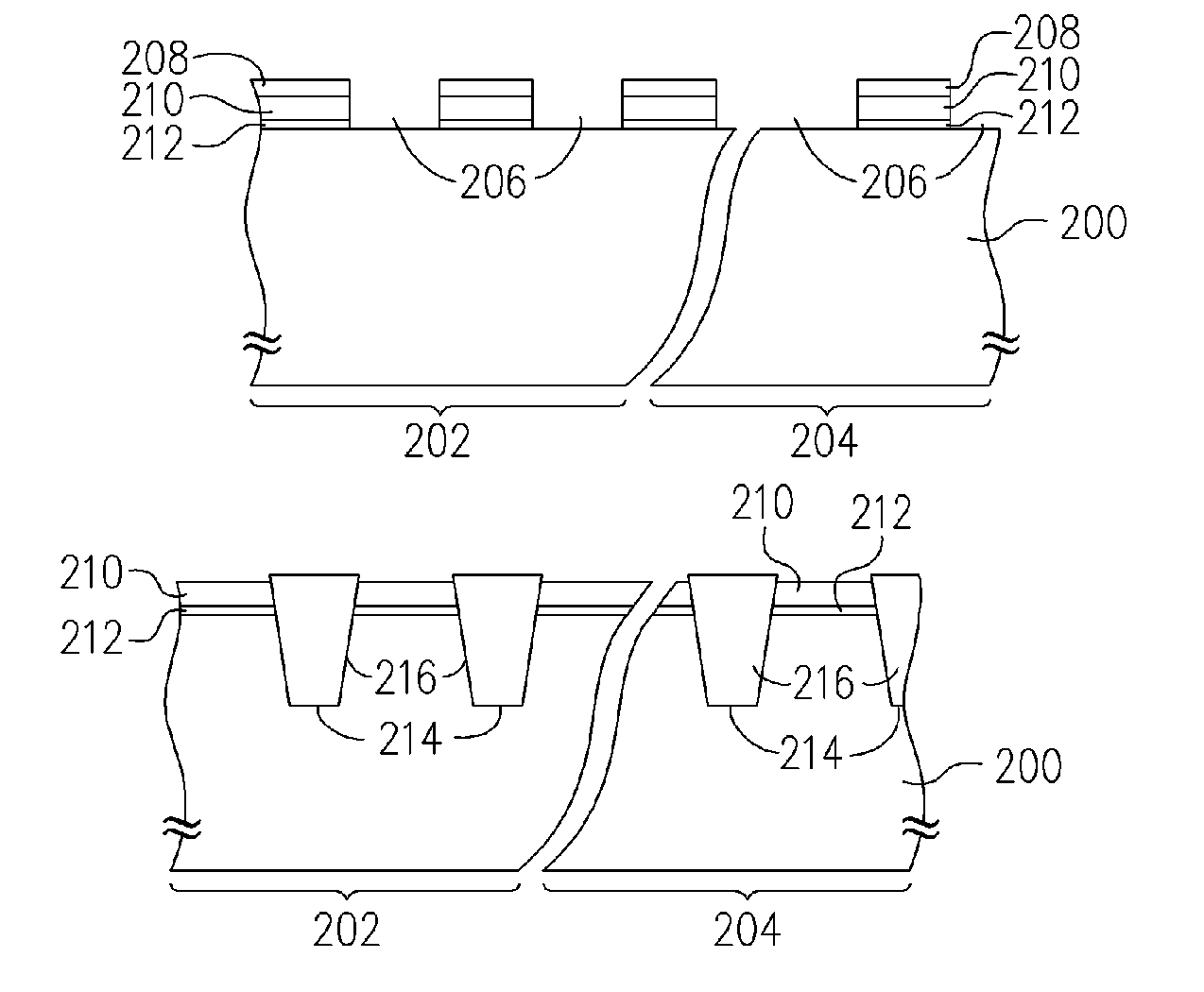
[0040]FIG. 2A to 2F are cross-sectional display views illustrating the fabrication process steps of a flash memory according to an embodiment of the present invention wherein FIG. 2E and 2F illustrates the same step in the fabrication flow and FIG. 2E is a cross-sectional display view of FIG. 2D along the sectional lines I-I′ and II-II′. FIG. 2F illustrates the step subsequent to the fabrication process step of FIG. 2E.

[0041] Referring to FIG. 2A, the substrate 200 is provided. The substrate 200 comprises a memory cell region 202 and the peripheral circuitry region 204. A dielectric material layer (not shown), a conductive material layer (not shown), and a mask layer (not shown) are formed sequentially on the substrate 200. The material of the dielectric material layer is, for example, silicon oxide, and the formation method thereof is, for example, thermal oxidation. The material of the conductive material layer is, for example, doped polysilicon, and the formation method thereof ...


PUM


Abstract

A fabrication method of a flash memory is provided. The substrate having a cell region and a peripheral circuitry region is provided. A patterned dielectric layer and a patterned conductive layer are formed on the substrate, and isolation structures are formed in the substrate. An inter gate dielectric layer and a poly layer are formed sequentially over the substrate. The poly layer and the inter gate dielectric in peripheral circuitry region are removed. After forming a second conductive layer and a mask layer over substrate, memory cells are formed in the cell region and a gate structure is formed in the peripheral circuitry region. A conductive plug is formed above the gate structure for electrically connecting the second conductive layer. Since the inter gate dielectric layer in the peripheral circuitry region is removed, the fabrication of the conductive plug can be simpler and the process window thereof can be improved.

Description

CROSS-REFERENCE TO RELATED APPLICATION [0001] This application claims the priority benefit of Taiwan application serial no. 94126670, filed on Aug. 8, 2005. All disclosure of the Taiwan application is incorporated herein by reference.BACKGROUND OF THE INVENTION [0002] 1. Field of Invention [0003] The present invention relates to a fabrication method of a semiconductor device, particularly, to a fabrication method of a flash memory. [0004] 2. Description of Related Art [0005] Memories are semiconductor devices used for storing information or data. As the microprocessors in computers become more powerful to be compatible with growingly massive amount of programs and calculations executed by the software, the capacities of the memories need to boost up. The developments of memories moves toward fabricating large-storage and low-cost memories to meet the requirements in semiconductor manufacture. [0006] Flash memory devices have been widely used as non-volatile memory devices in persona...

Claims


Application Information

Patent Timeline
Patent Type & Authority Applications(United States)
IPC IPC(8): H01L21/8234H01L21/336
CPCH01L27/115H01L27/11543H01L27/11526H10B41/40H10B41/48H10B69/00
Inventor LIU, SZU-HSIENWEI, HOUNG-CHI
Owner POWERCHIP SEMICON CORP
Why Eureka
Try Eureka