[0011]The method according to the invention uses an improved
optical alignment system for the orientation of a semiconductor wafer, said alignment
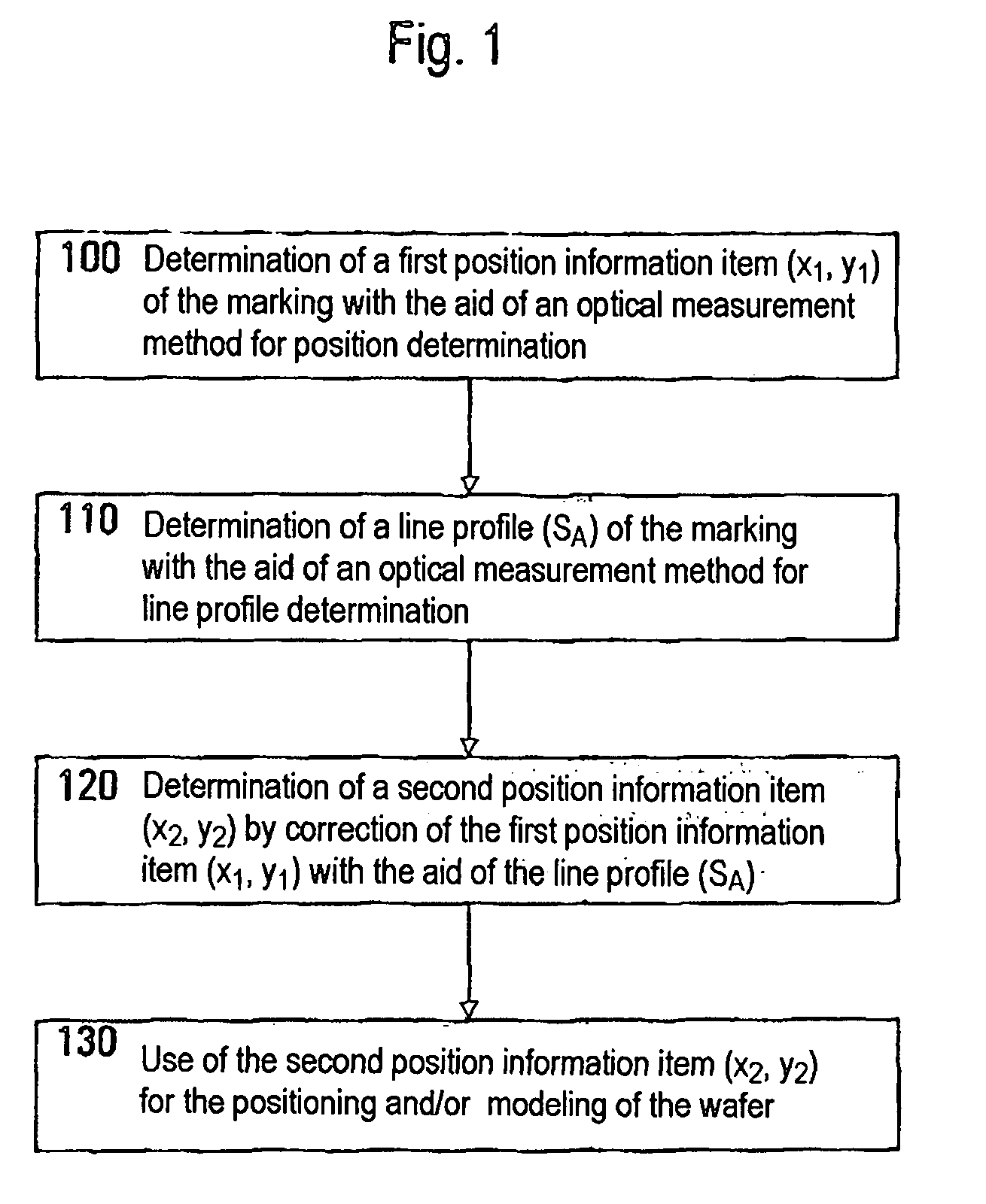
system providing a combination of two optical measurement methods. In this case, in a first step, a first position information item of an alignment mark arranged on the semiconductor wafer is determined with the aid of an optical measurement method that is optimized for position determination. In a further step, the determination of a line profile of the alignment mark in a predetermined direction takes place with the aid of an optical measurement method that is optimized for profile determination. According to the invention, the line profile of the alignment mark that is obtained in this case is used for correcting the first position information item obtained from the first step. The second position information item of the alignment mark that is determined by the correction is subsequently used for the positioning or the modeling of the semiconductor wafer. What is advantageous about the method according to the invention is that the combination of two optical measurement methods, one measurement method being optimized for the optical position determination and one measurement method being optimized for the optical profile determination of an alignment mark, enables the calculation of a particularly precise position information item. As a result of this, the semiconductor wafer can be oriented relative to a production tool more accurately than heretofore. An improved orientation of the semiconductor wafer relative to the production tool in turn brings about an improved
overlay accuracy of the structures of the different
layers and thus also larger process windows. Higher packing densities of the structures are possible, in principle, on account of the lower
overlay errors, as a result of which the performance of the semiconductor circuit can also be improved. A better overlay accuracy likewise results in a higher yield, and thus also contributes to lowering the fabrication costs.
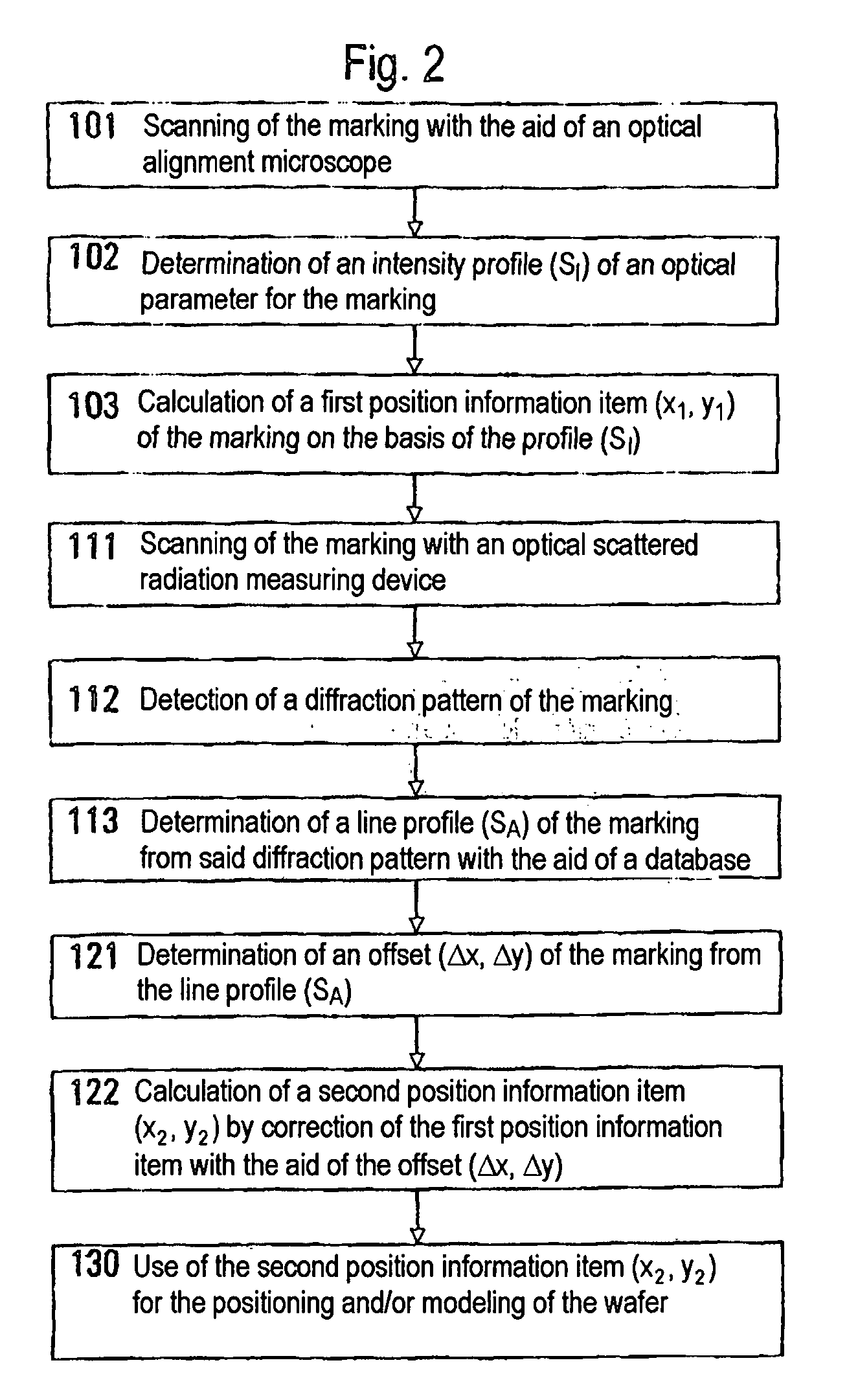
[0012]In one advantageous embodiment of the invention, the first position information items are determined with the aid of an
optical alignment microscope, the alignment mark being illuminated with light
radiation from a
light source and an optical parameter of the light
radiation, which is influenced by the alignment mark, being measured in a
spatially resolved manner in dependence on the relative position of the alignment mark with respect to the alignment
microscope. This is followed by the generation of an intensity profile of the optical parameter for the alignment mark in the predetermined direction, those relative positions of the alignment mark with respect to the alignment
microscope being determined in the case of which the optical parameter exceeds or falls below a predetermined threshold value. In the subsequent method step, the first position information item of the alignment mark is calculated with the aid of the intensity profile. This method, which is conventionally used for the alignment of a semiconductor wafer, has the
advantage that the first position information item can thereby generally be determined sufficiently rapidly, so that no unnecessary waiting times arise during the process.
[0013]It is particularly advantageous in this case to measure the intensity, the phase and / or the polarization of the light
radiation from a
light source that is influenced by the alignment mark. Measurements with the aid of these measurement methods can be carried out within a relatively short time, so that enough
process time remains for the subsequent steps of the method according to the invention.
[0014]In a further advantageous embodiment of the invention, the line profile of the alignment mark is determined with the aid of an optical scattered
radiation measuring device, the alignment mark being illuminated with light radiation from a
light source and a
diffraction pattern which arises as a result of the interaction of the light radiation with the regular structures of the alignment mark being detected. Afterward, the line profile of the alignment mark is determined on the basis of the
diffraction pattern with the aid of a
data processing device. What is advantageous in this case is that this method can be integrated within a conventional alignment system in a simple manner. With the aid of a
data processing device and through adjustment with
diffraction patterns in a
database, the profile determination can be carried out sufficiently rapidly by means of this method, so that, in this case, too, no waiting times have to be accepted. The use of the scattered
radiation measuring device furthermore makes it possible to determine the line profile of the regular structures of the alignment mark with a
high resolution. This enables a position determination and thus the orientation of the semiconductor wafer with a correspondingly high accuracy.
[0017]The use of at least two marks arranged spatially separated from one another on the semiconductor wafer enables the semiconductor wafer to be oriented two-dimensionally, it also being possible to detect rotations of the semiconductor wafer with respect to a predetermined orientation. Furthermore, it is also possible by this means to identify process-dictated distortions of the semiconductor wafer, which may arise e.g. on account of thermal or mechanical stress. By taking account of such distortions in the modeling of the semiconductor wafer, possible negative overlay effects resulting therefrom can largely be avoided.

