Overlay marks and semiconductor process using the overlay marks

Active Publication Date: 2016-10-20
UNITED MICROELECTRONICS CORP
View PDF0 Cites 7 Cited by
  • Summary
  • Abstract
  • Description
  • Claims
  • Application Information

AI Technical Summary

Benefits of technology

[0009]This invention will describe a novel configuration of correspondingly arranging and disposing the overlay/alignment marks based on their underlying patterns. The configur

Problems solved by technology

As the semiconductor industry has progressed into nanometer technology process nodes in pursuit of higher device density, higher performance, and lower costs, challenges from both fabrication and design issues have resulted in the development of three dimensional designs, such as a fin-like field effect transistor (FinFET).
Regardless of whether a mask is error-free, if all or part of the mask is not aligned properly, the resulting features may not align correctly with adjoining layers.
This can result in reduced device performance

Method used


Image

  • Overlay marks and semiconductor process using the overlay marks
  • Overlay marks and semiconductor process using the overlay marks
  • Overlay marks and semiconductor process using the overlay marks

Examples


Embodiment Construction

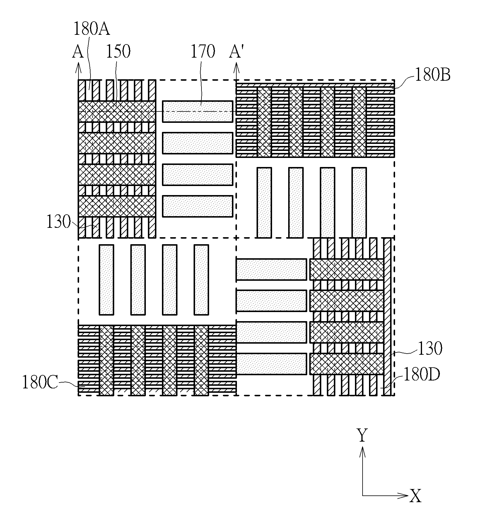
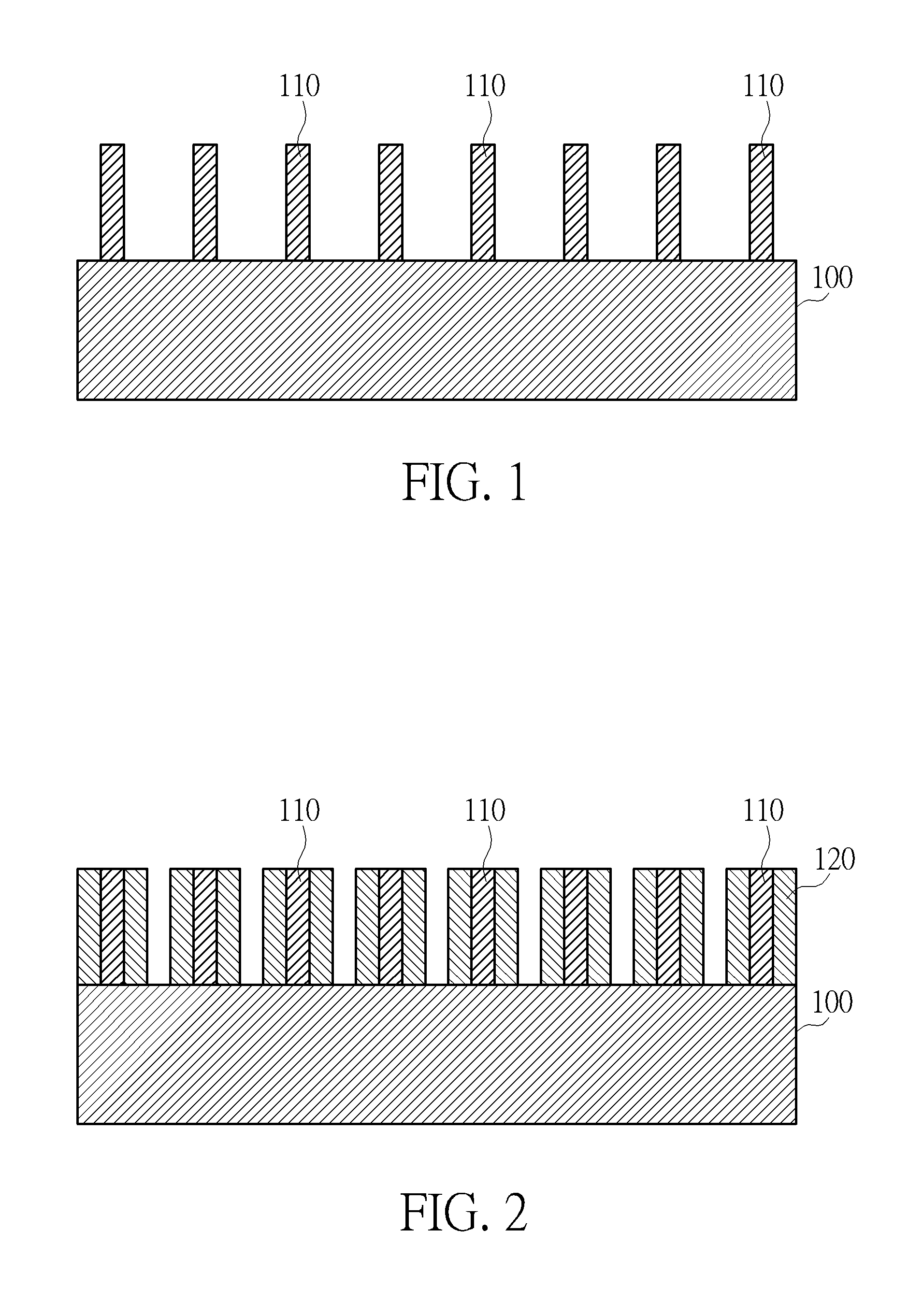
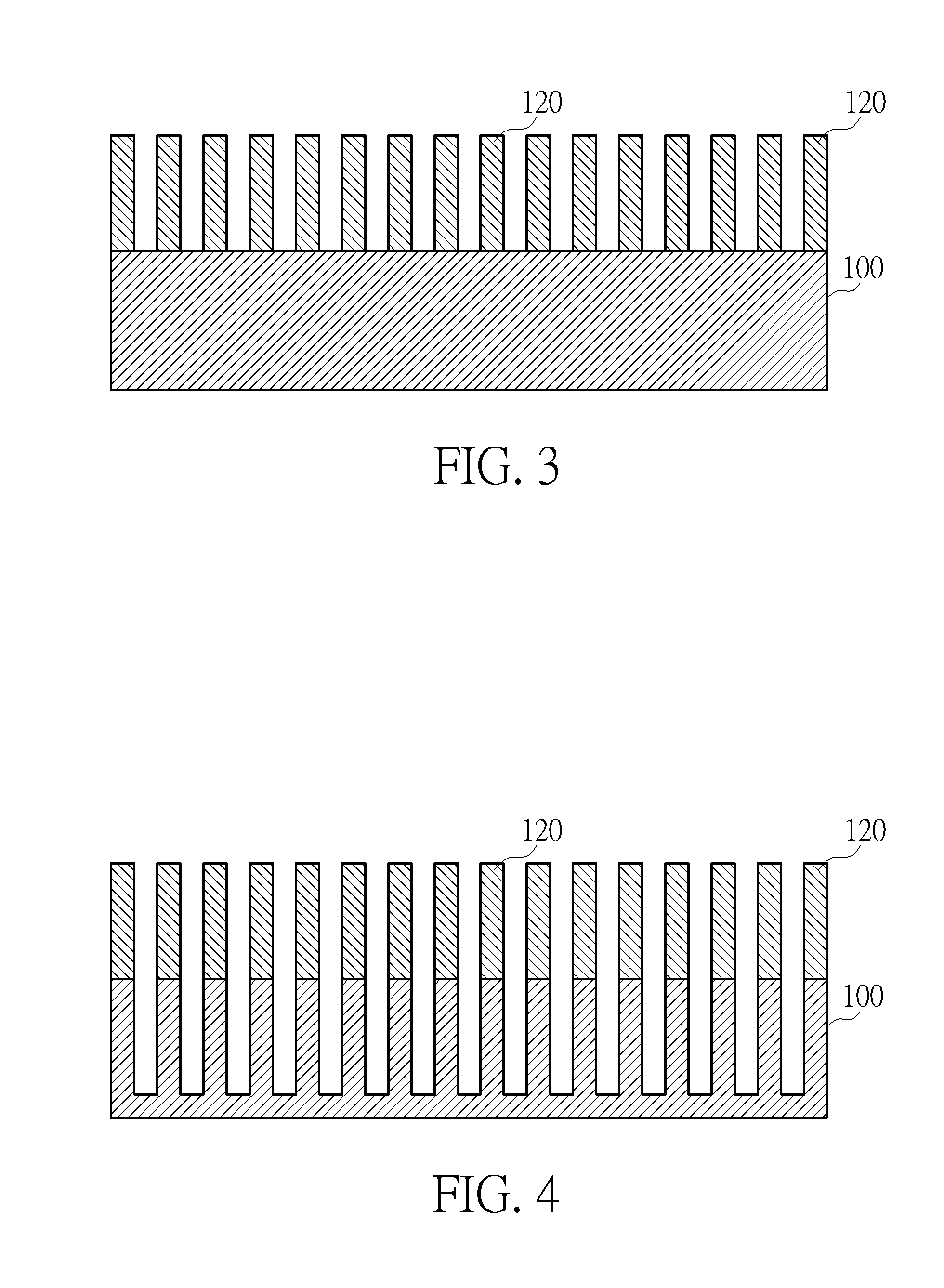
[0018]The present invention, in each of the various embodiments, uses overlay marks that are composed of periodic structures formed on each of two layers of a semiconductor wafer to provide overlay information between those two layers of the semiconductor device. The overlay marks are formed in specific locations on each wafer layer such that the periodic structures on one layer will be aligned with the periodic structures on the other layer when the two layers are properly aligned. Conversely, the periodic structures on each layer will be offset from each other when the two layers are not properly aligned. Alternatively, the present invention may use overlay marks that are composed of periodic structures formed on a single layer by two or more separate processes to provide alignment information between two different patterns on the same layer. Each of the periodic structures is composed of a plurality of structures, which increases the amount of information that may be used to meas...


PUM


Abstract

An overlay mark for determining the alignment between two separately generated patterns formed along with two successive layers above a substrate is provided in the present invention, wherein both the substrate and the overlay mark include at least two pattern zones having periodic structures with different orientations, and the periodic structures of the overlay mark are orthogonally overlapped with the periodic structures of the substrate.

Description

BACKGROUND OF THE INVENTION[0001]1. Field of the Invention[0002]The present invention relates generally to overlay measurement techniques, which are used in semiconductor manufacturing processes or system integration tests. More specifically, the present invention relates to overlay marks for measuring alignment error between different layers or different patterns on the same layer of a semiconductor wafer stack and the semiconductor process using the overlay marks.[0003]2. Description of the Prior Art[0004]As the semiconductor industry has progressed into nanometer technology process nodes in pursuit of higher device density, higher performance, and lower costs, challenges from both fabrication and design issues have resulted in the development of three dimensional designs, such as a fin-like field effect transistor (FinFET). A typical FinFET is fabricated with a thin “fin” (or fin structure) extending from a substrate, for example, etched into a silicon layer of the substrate. The...

Claims


Application Information

Patent Timeline
IPC IPC(8): H01L23/544H01L29/78
CPCH01L23/544H01L2223/5442H01L2223/54426H01L29/785G03F7/70633G03F7/70683H01L29/66795
Inventor LIN, CHIA-CHINGLIOU, EN-CHIUANWANG, CHIA-HUNGLEE, SHO-SHEN
Owner UNITED MICROELECTRONICS CORP
Why Eureka
Try Eureka