
Semiconductor laser element and near-field light output device using same

a laser element and semiconductor technology, applied in semiconductor lasers, electrical devices, laser details, etc., can solve the problems of inability to obtain desired near-field light, degrade the reliability of increase the amount of load on the semiconductor laser element, etc., to improve the yield of the near-field light output device, facilitate the alignment of the optical member, and reduce man-hours

Active Publication Date: 2016-11-03
SHARP FUKUYAMA LASER CO LTD
View PDF3 Cites 1 Cited by
  • Summary
  • Abstract
  • Description
  • Claims
  • Application Information

AI Technical Summary

Benefits of technology

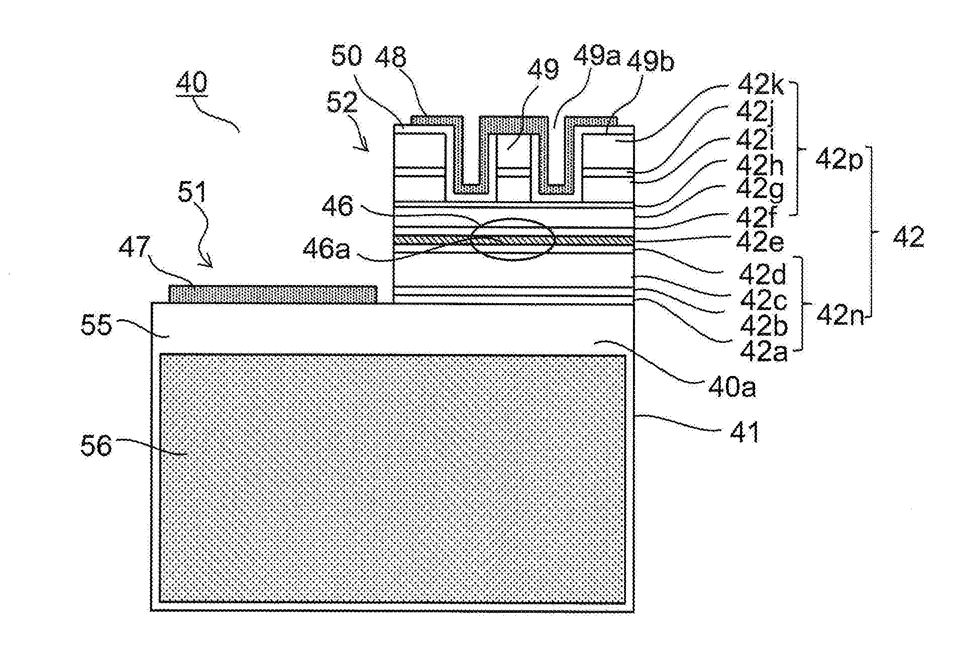
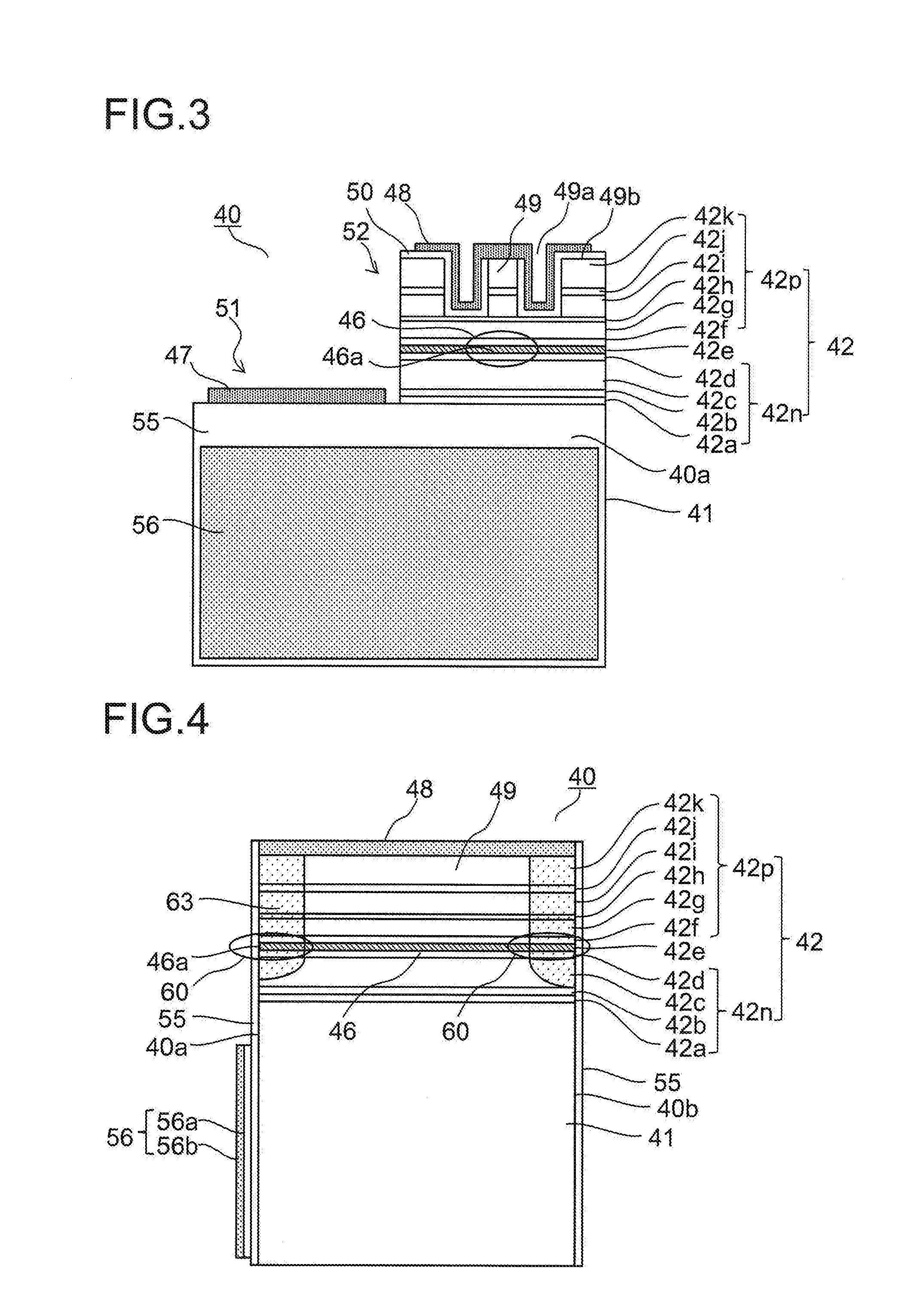
The present invention provides a semiconductor laser element with a first electrode and a second electrode that are disposed on one side with respect to a substrate, and one of two opposing surfaces perpendicular to an active layer is used as a fixing surface of the semiconductor laser element. This facilitates alignment of the optical member and the semiconductor laser element, helps reduce the man-hours of the near-field light output device, and helps improve the yield of the near-field light output device. This also helps achieve reduction of thermal resistance through reduction of connection surfaces.

Problems solved by technology

If output of laser light from the semiconductor laser element 40 is increased to overcome such reduction of laser light L, it increases amount of load on the semiconductor laser element 40, which leads to degraded reliability of the semiconductor laser element 40.
In addition, more heat is generated in the semiconductor laser element 40, and as a result, thermal distortion is caused, which changes a refractive index of the optical waveguide 15 of the slider 10, and this makes it impossible to obtain desired near-field light.
This causes problems of increased man-hours and reduced yield of the thermally-assisted magnetic recording head 1.

Method used


Image

  • Semiconductor laser element and near-field light output device using same
  • Semiconductor laser element and near-field light output device using same
  • Semiconductor laser element and near-field light output device using same

Examples


Embodiment Construction

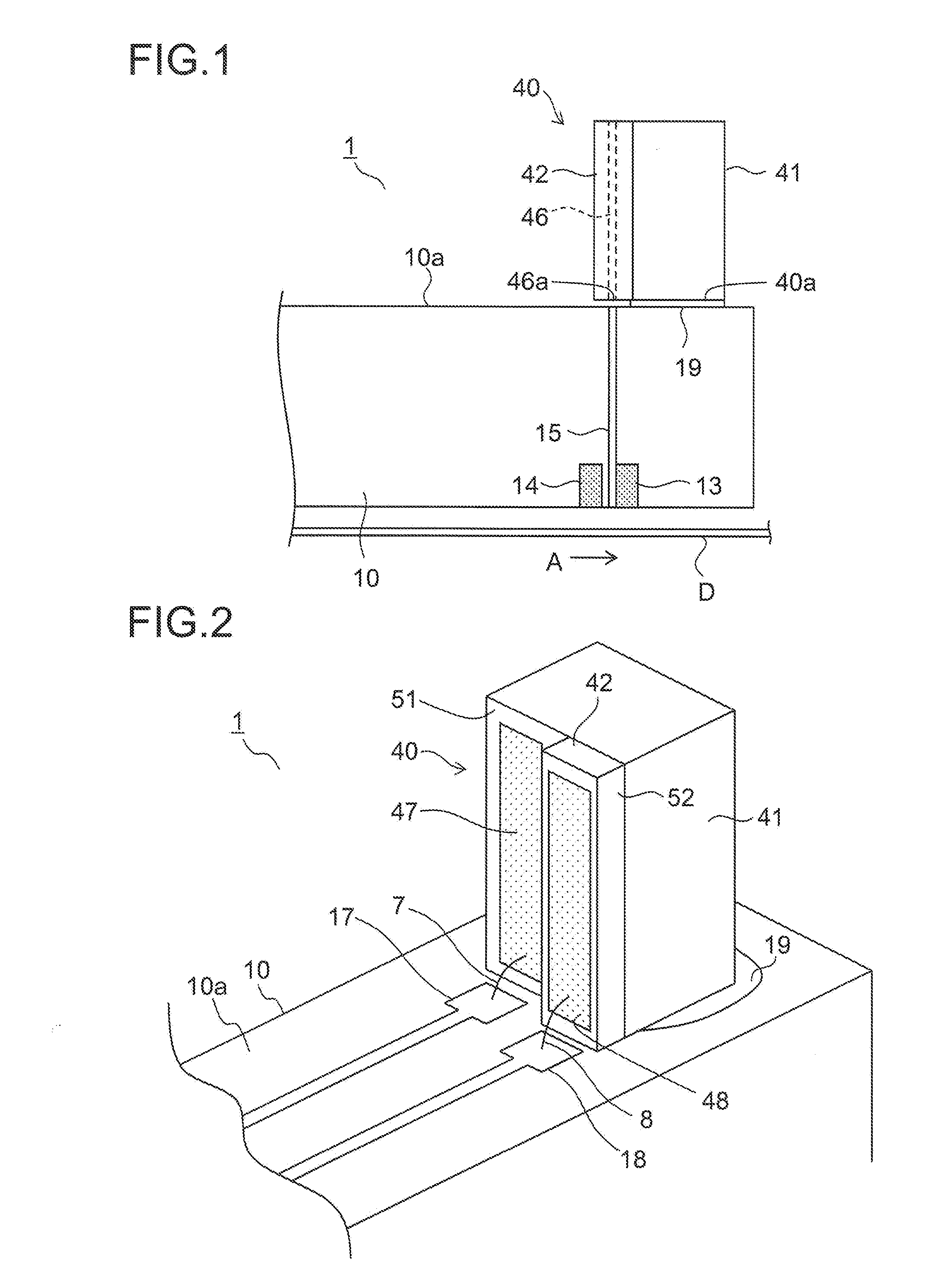
[0056]With reference to the accompanying drawings, embodiments of the present invention will be described below. For convenience of description, in the drawings referred to below, such portions as find their counter parts in the conventional example shown in FIG. 14 and FIG. 15 referred to above are denoted by common reference signs. FIGS. 1 and 2 are respectively a schematic front view of, and a perspective view showing a principal portion of, a thermally-assisted magnetic recording head as a near-field light output device of a first embodiment of the present invention.

[0057]A thermally-assisted magnetic recording head 1 is mounted in an HDD unit, for example, and is disposed by being supported by a suspension (not shown) so as to be movable in an axial direction over a magnetic disk D. The thermally-assisted magnetic recording head 1 includes a slider 10 (an optical member) which faces the magnetic disk D, and a semiconductor laser element 40 which is fixed to the slider 10 by a f...


PUM


Abstract

A semiconductor laser element is provided with: a substrate formed of a semiconductor; a semiconductor laminated film, which is laminated on the substrate, and which includes an active layer; a first electrode and a second electrode, which are provided on surfaces parallel to the active layer on the side where the semiconductor laminated film is formed on the substrate; and a facet protection film that is provided on both the facets, which are perpendicular to the active layer, and which face each other. In the semiconductor laser element, the facet is used as a fixing surface for the semiconductor laser element, said facet having the facet protection film formed thereon.

Description

CROSS-REFERENCE TO RELATED APPLICATIONS[0001]This application is a U.S. National Phase patent application of International Patent Application No. PCT / JP2014 / 072414, filed on Aug. 27, 2014, which claims priority to Japanese Application No. 2013-240971, filed on Nov. 21, 2013, each of which is hereby incorporated by reference in the present disclosure in its entirety.FIELD OF THE INVENTION[0002]The present invention relates to a semiconductor laser element having a two-electrode-at-one-side structure, and a near-field light output device using the same.BACKGROUND OF THE INVENTION[0003]Recently, in the fields of laser processing and large capacity storage, near-field light has come to be used to achieve microfabrication and high-density recording, etc., which have conventionally been impossible due to light diffraction limit. A near-field light output device configured to output near-field light directs laser light to an optical waveguide where a near-field light generating element is ...

Claims


Application Information

Patent Timeline
IPC IPC(8): H01S5/028H01S5/02H01S5/22H01S5/022
CPCH01S5/028H01S5/22H01S5/0208H01S5/02256H01S5/162H01S5/02345H01S5/02355H01S5/042
Inventor TANI, KENTAROHKAWAKAMI, TOSHIYUKIARIYOSHI, AKIRA
Owner SHARP FUKUYAMA LASER CO LTD
Learn More