Eureka AIR delivers breakthrough ideas for toughest innovation challenges, trusted by R&D personnel around the world.

Array substrate and manufacturing method thereof, display device

Active Publication Date: 2016-11-10
BOE TECH GRP CO LTD +1
View PDF33 Cites 8 Cited by
  • Summary
  • Abstract
  • Description
  • Claims
  • Application Information

AI Technical Summary

Benefits of technology

The present invention allows for the antenna to be integrated directly into the display panel, reducing the area of the circuit board and utilizing the spare area of the array substrate, ultimately improving the integration level and reducing the overall size of the display device. Additionally, the antenna can be prepared on a glass substrate, which improves the quality of the antenna due to the insulating properties of the substrate.

Problems solved by technology

However, the integration of some passive devices is not as simple as active devices.
However, since the semiconductor property of the silicon based substrate may result in substrate loss when the antenna works, and the antenna occupies a relatively large area of the silicon based substrate, development of a wireless communication terminal that is light and thin is limited by the use of the antenna on the silicon based substrate to some extent.

Method used


Image

  • Array substrate and manufacturing method thereof, display device
  • Array substrate and manufacturing method thereof, display device
  • Array substrate and manufacturing method thereof, display device

Examples


Embodiment Construction

[0031]Specific embodiments of the present invention will be described in greater detail with reference to the drawings and the embodiments. The following embodiments are for explanatory purposes only and not for limiting the scope of the present invention.

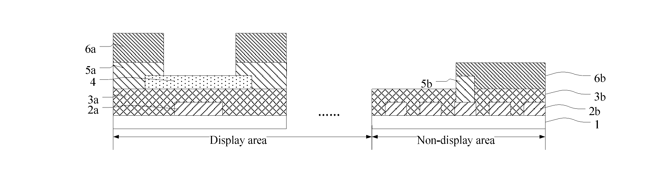
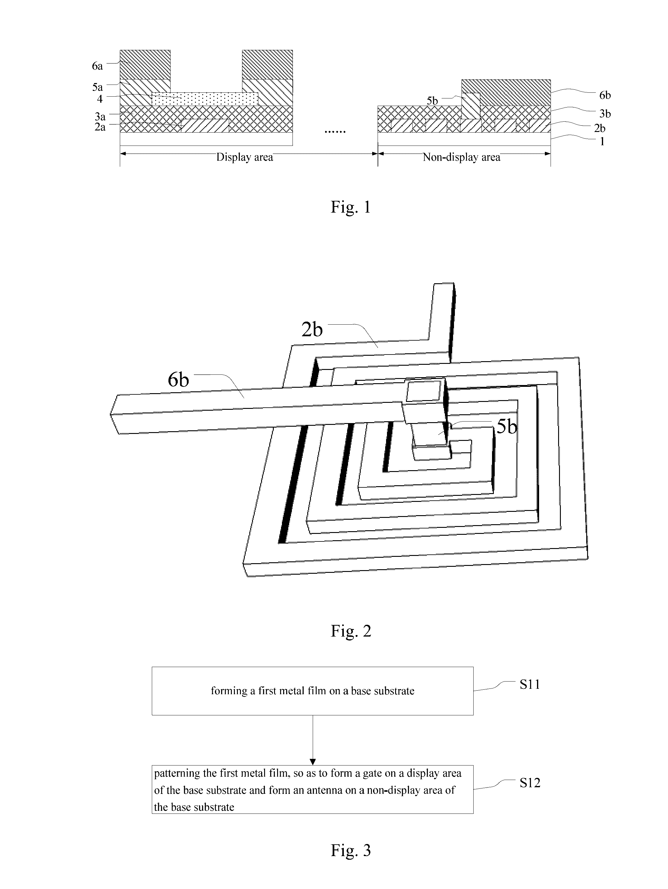
[0032]An embodiment of the present invention provides an array substrate, the array substrate comprising a base substrate, and a gate, a gate insulating layer, an active layer and a source / drain arranged on the base substrate, the array substrate further comprising an antenna for receiving and / or transmitting wireless signals, with the antenna arranged on the base substrate.

[0033]FIG. 1 is a schematic view of an array substrate provided by an embodiment of the present invention. The array substrate comprises a base substrate 1, a gate 2a, a gate insulating layer 3a, an active layer 4 and a source / drain 6a are arranged successively on a display area of the base substrate 1. Optionally, a buffer metal layer 5a can also be arranged be...


PUM


Abstract

An array substrate and a manufacturing method thereof, comprising a base substrate, and a gate, a gate insulating layer, an active layer and a source / drain arranged on the base substrate, the array substrate further comprising an antenna for receiving and / or transmitting wireless signals, the antenna being arranged on the base substrate. By arranging the antenna on the base substrate of the array substrate, the antenna is integrated directly in the display panel. Thus, not only the area of the PCB circuit board in the display device can be reduced, but also the spare area in the array substrate can be utilized sufficiently, thereby improving the integration level of the display device and reducing the total volume of the display device.

Description

RELATED APPLICATIONS[0001]The present application is the U.S. national phase entry of PCT / CN2015 / 084192,with an international filing date of Jul. 16, 2015, which claims the benefit of Chinese Patent Application No. 201410785115.6, filed on Dec. 16, 2014, the entire disclosures of which are incorporated herein by reference.FILED OF THE INVENTION[0002]The present invention relates to the field of display, particularly to an array substrate and manufacturing method thereof, and a display device.BACKGROUND OF THE INVENTION[0003]With development of the microelectronic technology, various sensors can be integrated through the microelectronic technique, in which the integrated devices represented by silicon based micro electro mechanical technology are particularly prominent. However, the conventional silicon based device is still an independent physical module in system level design, which may impact on improving integration level of the whole system and reducing the volume.[0004]In the c...

Claims


Application Information

Patent Timeline
IPC IPC(8): H01L27/13H01L27/12
CPCH01L27/13H01L2021/775H01L27/1262H01L27/124H01L23/5227G02F1/136286G02F1/133388H01L21/77H01L23/645
Inventor HE, ZONGZEWANG, JIANMINGMENG, ZHIMINGHU, WEIHAO
Owner BOE TECH GRP CO LTD
Why Eureka
Eureka Blog
Learn More