Semiconductor device

a technology of mikro-onductors and capacitors, which is applied in the direction of mikro-onductors, basic electric elements, electrical apparatus, etc., can solve the problems of inability to maintain an even potential distribution in the withstand region, the adverse effect of movable ions or charge of mold resin on the breakdown voltage characteristics of high voltage ic, and the inability to reduce the capacity so as to suppress the voltage drop amount of the bootstrap capacitor, the effect of reducing

Active Publication Date: 2014-08-07
FUJI ELECTRIC CO LTD
View PDF4 Cites 21 Cited by
  • Summary
  • Abstract
  • Description
  • Claims
  • Application Information

AI Technical Summary

Benefits of technology

[0061]According to the invention, it is possible, by connecting one end portion of the resistive thin film layer to the first electrode and the other end portion of the resistive thin film layer to the third electrode, to generate successive voltage drop from the potential of the third electrode, which is the negative electrode side potential of the bootstrap capacitor, to the potential of the first electrode, which is the ground potential. Because of this, it is possible to maintain an even potential distribution between the first electrode and third electrode. Because of this, compared to the heretofore known high voltage IC, it is possible to suppress the voltage drop amount of the bootstrap capacitor caused by a discharge from the bootstrap capacitor to the ground occurring during the on-state period of an upper arm output power device of an output power device configuring, for example, a PWM inverter bridge circuit.
[0062]Also, as it is possible to suppress the voltage drop amount of the bootstrap capacitor more than in the heretofore known high voltage IC, it is possible to reduce the capacity of the bootstrap capacitor compared to that of the heretofore known high voltage IC. Because of this, it is possible to configure the bootstrap capacitor with only a small electronic part such as, for example, a ceramic capacitor, and thus possible to achieve a reduction in PCB area. Also, as it is also possible to reduce the voltage drop amount of the bootstrap capacitor when the upper arm output power device is switching, it is possible to maintain the drive capability of the upper arm output power device.
[0063]According to the invention, by providing a resistive thin film layer whose two end portions are connected one each to the first electrode and third electrode in a semiconductor device including a diode structure and a semiconductor device including a transistor structure, it is possible to even the potential distribution in a withstand region formed of the semiconductor device including a diode structure and semiconductor device including a transistor structure. Because of this, it is possible to achieve an increase in the long term reliability of a high temperature bias test, and the like.
[0064]According to the semiconductor device according to the invention, an advantage is achieved in that it is possible to maintain the reliability of a high voltage IC. Also, according to the semiconductor device according to the invention, an advantage is achieved in that it is possible to increase breakdown voltage. Also, according to the semiconductor device according to the invention, an advantage is achieved in that it is possible to reduce cost.

Problems solved by technology

However, when the breakdown voltage guaranteed in the withstand region is extremely high, such as in a high voltage IC of, for example, a 1,200 V breakdown voltage class, it is necessary that the impurity concentration of the withstand region be extremely low.
However, due to the impurity concentration of the withstand region surface being low, and the voltage applied to the high voltage IC being high, the adverse effect on the breakdown voltage characteristics of the high voltage IC caused by movable ions or charge of the mold resin is even more noticeable.
In this case, the movable ions or charge of the mold resin accumulate on a protective film of the high voltage IC, because of which, with a capacitive field plate structure, it is not possible to maintain an even potential distribution in the withstand region with respect to the amount of movable ions or charge accumulated on the protective film on the withstand region.
Because of this, when the breakdown voltage guaranteed in the withstand region is extremely high, or when the amount of charge contained in the mold resin is extremely large, it is often the case that the resistive field plate structure is applied such that deterioration in breakdown voltage characteristics due to movable ions or charge in the mold resin is unlikely to occur.
However, a problem occurs in that the PCB (Printed Circuit Board) area of an inverter power supply system will be increased by increasing the capacity of an electrolytic capacitor (approximately several μF).
Also, by reducing the on-state period of upper arm IGBT 17, the standard width between the minimum on-state time t1 and maximum on-state time t2 narrows, and a problem occurs in that the operation of the high voltage IC is restricted.
However, when disposing the high resistance polysilicon thin film with the heretofore described dimensions (1 μm width and 1 μm interval) or lower, the following kinds of problem occur.
For example, when reducing the width of the high resistance polysilicon thin film, problems occur with processing accuracy in the manufacturing process in that it is difficult to optimize resist exposure conditions when patterning the high resistance polysilicon thin film, the high resistance polysilicon thin film becomes detached when etching the high resistance polysilicon thin film, and the like.
Because of this, realistically, it is also difficult to reduce the disposition area of the high resistance polysilicon thin film.
However, it is necessary to optimize the high breakdown voltage device structure in order to increase the width of the withstand region of the high breakdown voltage junction termination region, and the chip area also increases, which is not desirable as the cost increases considerably.
Consequently, it is necessary to add a photolithography step, an ion implantation step, and the like, exclusively for forming a low impurity concentration high resistance polysilicon thin film on resistive field plate structure portion 1401, and there is a problem in that the manufacturing cost increases.

Method used


Image

  • Semiconductor device
  • Semiconductor device
  • Semiconductor device

Examples


embodiment 1

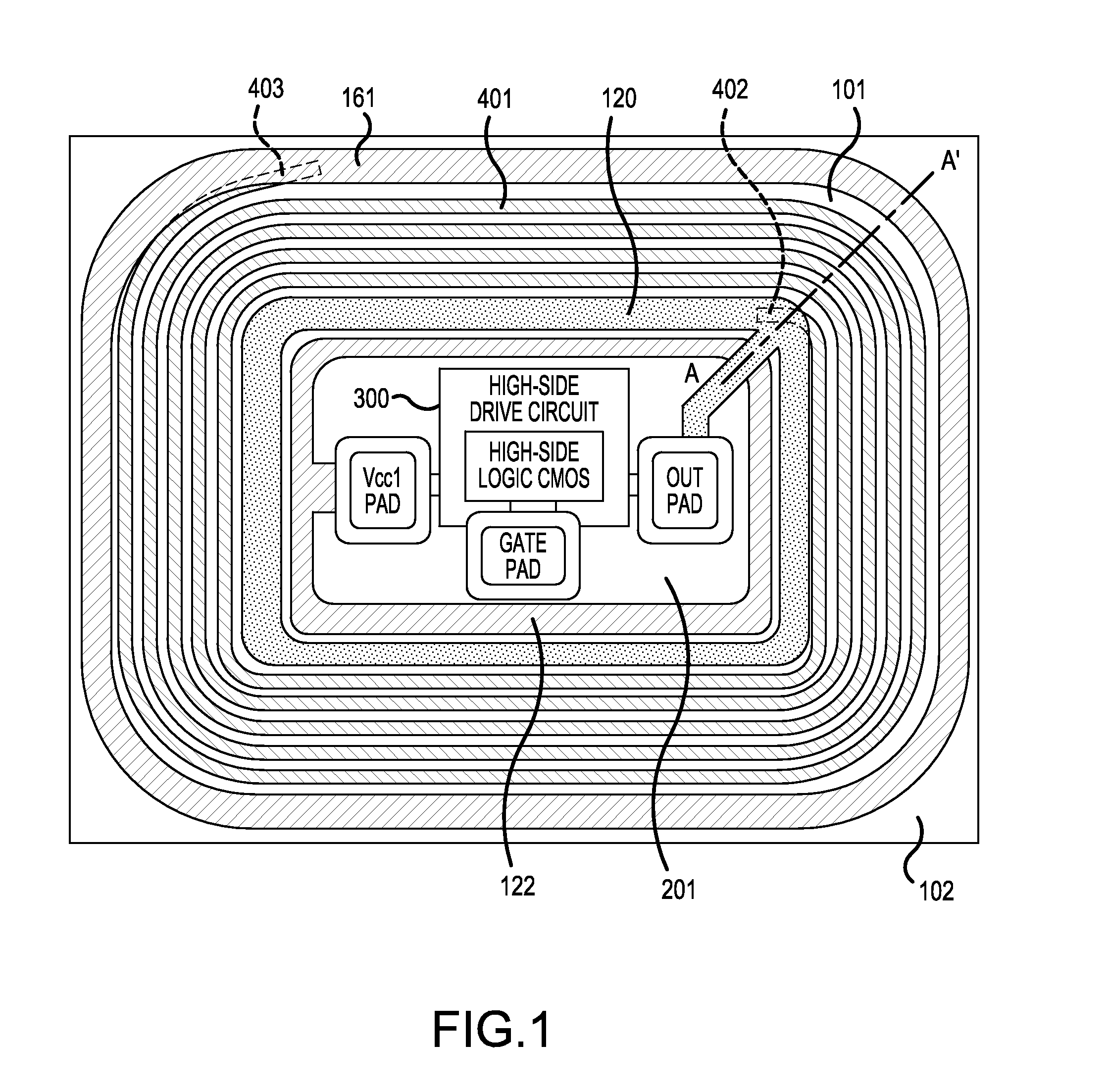
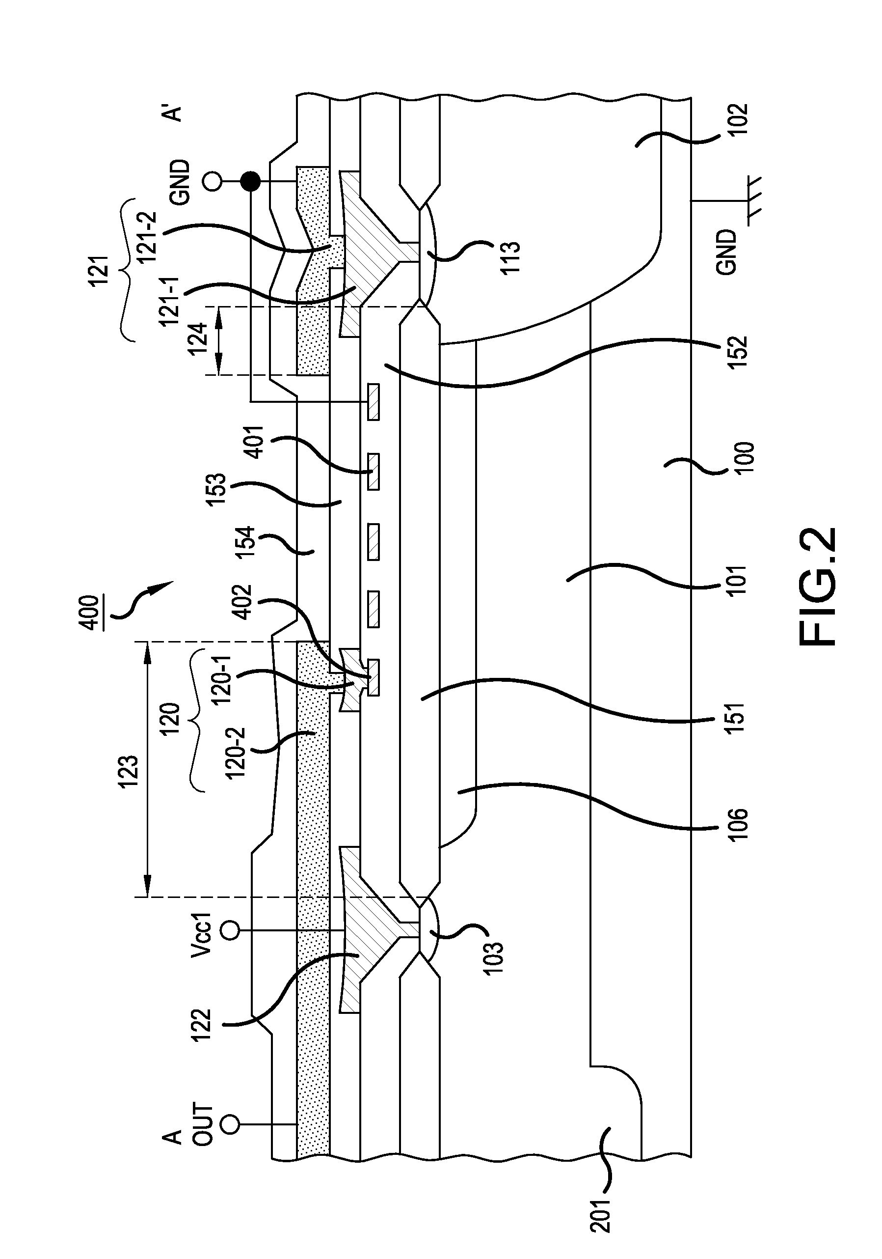
[0086]A description will be given of a high voltage IC according to Embodiment 1, using FIGS. 1, 2, and 16. FIG. 1 is a plan view showing a main portion of a high voltage IC according to Embodiment 1. Also, FIG. 2 is a sectional view showing a sectional structure along a cutting plane line A-A′ in FIG. 1. FIG. 1 shows a high-side drive circuit 300 and main portions of a high breakdown voltage junction termination region (HVJT) 400 in the high voltage IC according to Embodiment 1. As shown in FIG. 1, n-type well region 201, n− type region (a second conductivity type well region) 101, and p-type well region (a first conductivity type well region) 102 are disposed on a p− type silicon substrate (a first conductivity type semiconductor layer, not shown).

[0087]N-type well region 201 is a region (hereafter referred to as a high potential region) with a potential higher than that of other regions partitioned off by p-type well region 102. High-side drive circuit 300, an OUT pad, a gate pad...

embodiment 2

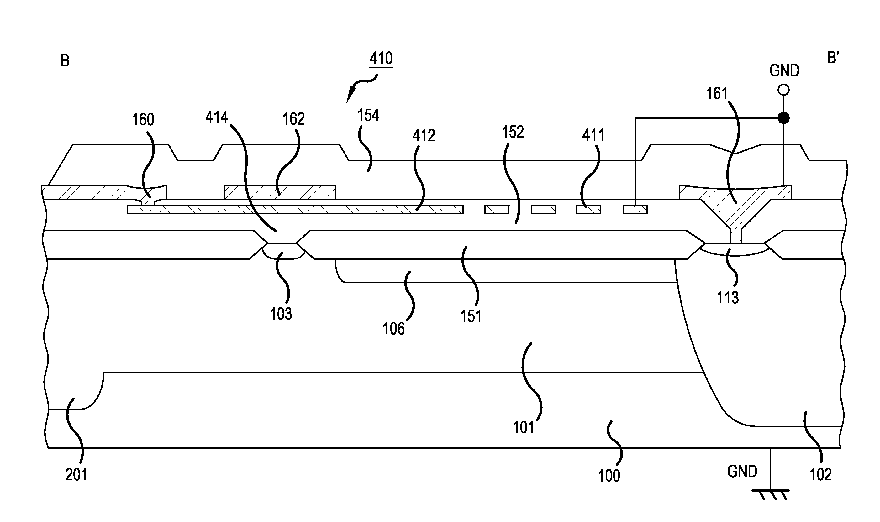
[0134]FIG. 4 is a plan view showing a main portion of a high voltage IC according to Embodiment 2. Also, FIG. 5 is a sectional view showing a sectional structure along a cutting plane line B-B′ in FIG. 4. FIG. 6 is a sectional view showing a sectional structure along a cutting plane line C-C′ in FIG. 4. FIG. 4 shows high-side drive circuit 300 and main portions of a high breakdown voltage junction termination region 410 in the high voltage IC according to Embodiment 2. The high voltage IC according to Embodiment 2 differs from Embodiment 1 in that first contact portion 412 of a high resistance polysilicon thin film 411 configuring a resistive field plate structure is connected to OUT electrode 160 formed of a first metal layer.

[0135]As shown in FIGS. 4 to 6, the high voltage IC according to Embodiment 2 is such that OUT electrode 160 is disposed on n-type well region 201. OUT electrode 160, being configured of only the first metal layer, does not have an upper layer electrode formed...

embodiment 3

[0141]FIG. 7 is a plan view showing a main portion of a high voltage IC according to Embodiment 3. Also, FIG. 8 is a sectional view showing a sectional structure along a cutting plane line D-D′ in FIG. 7. FIG. 7 shows high-side drive circuit 300 and main portions of high breakdown voltage junction termination region 420 in the high voltage IC according to Embodiment 3. A sectional structure along a cutting plane line E-E′ in FIG. 7 is the same as the sectional structure shown in FIG. 6. The high voltage IC according to Embodiment 3 is a modification example of the high voltage IC according to Embodiment 2. The high voltage IC according to Embodiment 3 differs from Embodiment 2 in that, in portion 424 in which pickup contact portion 413 is not provided, no Vcc1 electrode 172 is provided either.

[0142]As shown in FIGS. 7 and 8, the high voltage IC according to Embodiment 3 is such that Vcc1 electrode 172, in the same way as pickup contact portion 413, has a ring-like planar form wherei...


PUM


Abstract

An n-type region encloses an n-type well region is disclosed in which is disposed a high-side drive circuit. A high resistance polysilicon thin film configuring a resistive field plate structure of a high breakdown voltage junction termination region is disposed in spiral form on the n-type region. An OUT electrode, a ground electrode, and a Vcc1 electrode are disposed on the n-type region. The Vcc1 electrode is connected to the positive electrode of an auxiliary direct current power supply (a bootstrap capacitor). The OUT electrode is connected to the negative electrode of the auxiliary direct current power supply. One end portion (a second contact portion) of the high resistance polysilicon thin film is connected to the ground electrode, and the other end portion (a first contact portion) of the high resistance polysilicon thin film is connected to the OUT electrode.

Description

BACKGROUND OF THE INVENTION[0001]A. Field of the Invention[0002]The present invention relates to a semiconductor device.[0003]B. Description of the Related Art[0004]As well as motor-controlling inverters, power devices are widely utilized in a large number of fields, such as large capacity PDPs (plasma display panels), power supply applications for FDPs (flat panel displays) such as liquid crystal panels, and inverters for domestic electrical appliances such as air conditioners or lighting. IGBTs (insulated gate bipolar transistors) and power MOSFETS (insulated gate field effect transistors) are known as this kind of power device.[0005]To date, the drive and control of a power device has been carried out using an electronic circuit configured by combining a semiconductor device such as a photocoupler and an electronic part such as a transformer. However, owing to recent advances in LSI (large scale integrated circuit) technology, power devices are being used in 100 V AC (alternating...

Claims


Application Information

Patent Timeline
Patent Type & Authority Applications(United States)
IPC IPC(8): H01L29/739
CPCH01L29/7393H01L21/765H01L27/0922H01L29/0634H01L29/0696H01L29/405H01L29/42368H01L29/7395H01L29/7816H01L29/7835H01L29/8611
Inventor YAMAJI, MASAHARU
Owner FUJI ELECTRIC CO LTD
Why Eureka
Try Eureka