Eureka AIR delivers breakthrough ideas for toughest innovation challenges, trusted by R&D personnel around the world.

Semiconductor structure and method for manufacturing the same

Active Publication Date: 2012-12-27
INST OF MICROELECTRONICS CHINESE ACAD OF SCI
View PDF1 Cites 8 Cited by
  • Summary
  • Abstract
  • Description
  • Claims
  • Application Information

AI Technical Summary

Benefits of technology

[0006]The object of the present disclosure is to provide semiconductor structures and methods for manufacturing the same, to overcome the foregoing problems in the prior art, such that the threshold voltages of the pMOSFET and the nMOSFET can be adjusted respectively and the integration level can be improved.
[0009]According to the embodiments of the semiconductor structure and method for manufacturing the same of the present disclosure, the counter-doped region is formed in the backgate structure formed in the buried semiconductor layer in such a manner that the counter-doped region is self-aligned with the gate electrode. The threshold voltages of different MOSFETs can be adjusted by the backgate. In the case that both the pMOSFET and the nMOSFET are formed in one semiconductor structure, the threshold voltages of different semiconductor devices can be varied by the counter-doped region. Thus, the threshold voltages of the pMOSFET and nMOSFET can be adjusted respectively by one backgate contact, which greatly improves the integration level of the semiconductor device.

Problems solved by technology

Consequently, the backgate contacts occupy an increased footprint, which hinders further improvement of the integration level of a semiconductor device.

Method used


Image

  • Semiconductor structure and method for manufacturing the same
  • Semiconductor structure and method for manufacturing the same
  • Semiconductor structure and method for manufacturing the same

Examples


Embodiment Construction

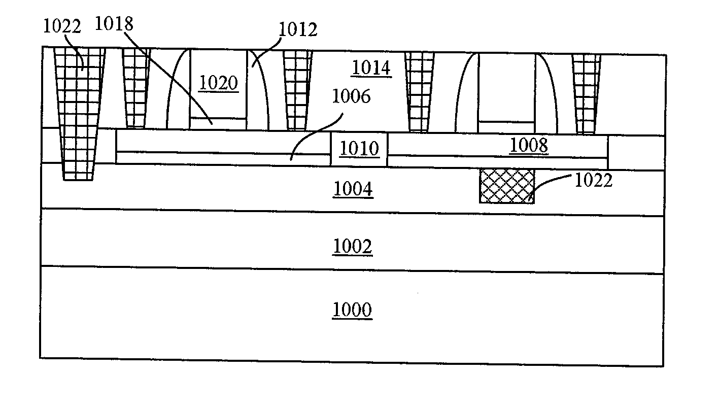
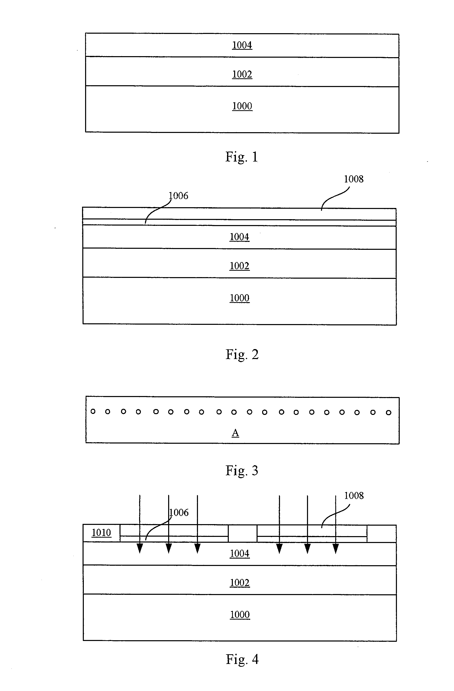
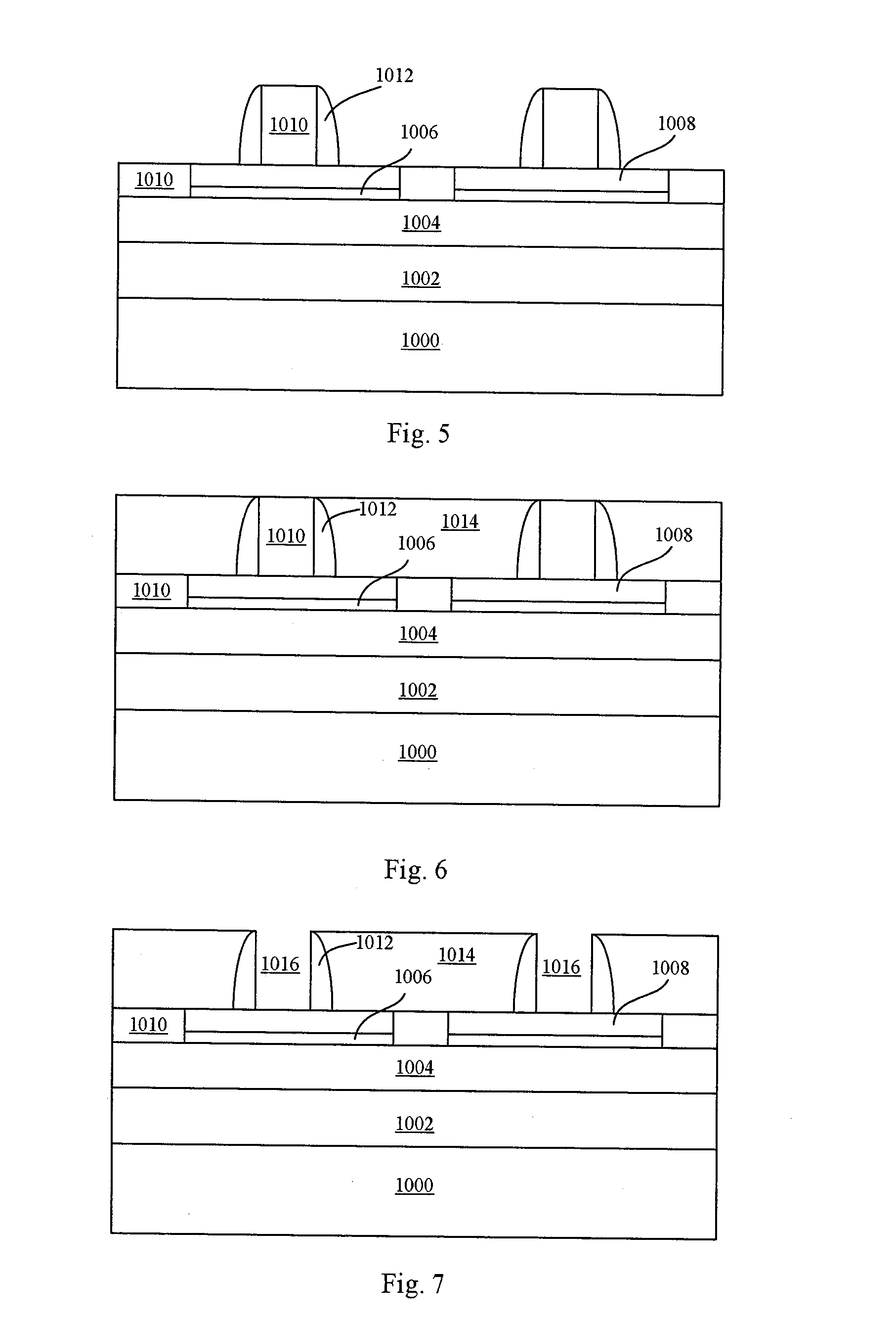
[0012]Exemplary embodiments of the present disclosure will be described in more details below with reference to the accompanying drawings. However, it should be understood that the description of the embodiments of the present disclosure is illustrative and is not intended to limit the scope of the disclosure. In addition, those well known structures and technology are omitted thereinafter, for the sake of avoiding unnecessary confusion to the conception of the present disclosure.

[0013]Layered structures according to the embodiments of the present disclosure are schematically shown in the accompanying drawings. The figures are provided only for illustration and not drawn to scale, in which some details are exaggerated, and some other details are probably omitted, for the sake of clarity. Shapes, relative sizes and relative positions of various regions and layers shown in the figures are only illustrative, and can be varied actually because of manufacturing tolerance or technical lim...


PUM


Abstract

The present application discloses a semiconductor structure and method for manufacturing the same. The semiconductor structure comprises: an SOI substrate and a MOSFET formed on the SOI substrate, wherein the SOI substrate comprises, in a top-down fashion, an SOI layer, a first buried insulator layer, a buried semiconductor layer, a second buried insulator layer, and a semiconductor substrate, the buried semiconductor layer including a backgate region including a portion of the buried semiconductor layer doped with a dopant of a first polarity; the MOSFET comprises a gate stack and source / drain regions, the gate stack being formed on the SOI layer, and the source / drain regions being formed in the SOI layer at opposite sides of the gate stack; and the backgate region includes a counter-doped region, the counter-doped region is self-aligned with the gate stack and includes a dopant of a second polarity, and the second polarity is opposite to the first polarity. The embodiment of the present disclosure can be used for adjusting a threshold voltage of a MOSFET.

Description

CROSS-REFERENCE TO RELATED APPLICATION(S)[0001]This application claims priority to the Chinese Patent Application No. 201110173892.1, filed on Jun. 24, 2011, which is incorporated herein by reference in its entirety.TECHNICAL FIELD[0002]The present disclosure relates to semiconductor manufacturing technology, and more particularly, to semiconductor structures formed in an ultrathin Semiconductor on Insulator (SOI) and methods for manufacturing the same.BACKGROUND[0003]As a dimension of a semiconductor device becomes smaller continuously, a key size of the semiconductor device, i.e. a gate length, becomes shorter continuously. When the gate length of a metal oxide semiconductor field effect transistor (MOSFET) decreases to below 45 nm, the MOSFET exhibits more significant short channel effects (SCE). The short channel effects include threshold voltage drift, lower carrier mobility, Drain Induced Barrier Lowering (DIBL), and other effects of the semiconductor device.[0004]One known ap...

Claims


Application Information

Patent Timeline
IPC IPC(8): H01L29/772H01L21/336
CPCH01L21/823828H01L21/823878H01L21/84H01L27/1203H01L29/78603H01L29/78612H01L29/4908
Inventor ZHU, HUILONGLIANG, QINGQINGLUO, ZHIJIONGYIN, HAIZHOU
Owner INST OF MICROELECTRONICS CHINESE ACAD OF SCI
Why Eureka
Eureka Blog
Learn More