OLED package structure and packaging method

a technology of organic light-emitting diodes and packaging, which is applied in the field of packaging technology, can solve the problems of affecting the life of oled devices, unable to provide a sufficient mechanical strength, and inability to meet the requirements of oled display panels of large sizes, and achieves excellent packaging effect, excellent blocking ability of moisture and oxygen, and high mechanical strength

Active Publication Date: 2016-11-24
SHENZHEN CHINA STAR OPTOELECTRONICS TECH CO LTD
View PDF14 Cites 6 Cited by
  • Summary
  • Abstract
  • Description
  • Claims
  • Application Information

AI Technical Summary

Benefits of technology

[0008]An object of the present invention is to provide an OLED package structure, which has an excellent capability of blocking moisture and oxyg...

Problems solved by technology

Electrochemical corrosion may readily occur in a humid environment so as to severely affect the lifespan of an OLED device.
However, the frit based laser packaging process generally needs the gap of a cavity to be large, making it impo...

Method used


Image

  • OLED package structure and packaging method
  • OLED package structure and packaging method
  • OLED package structure and packaging method

Examples


Embodiment Construction

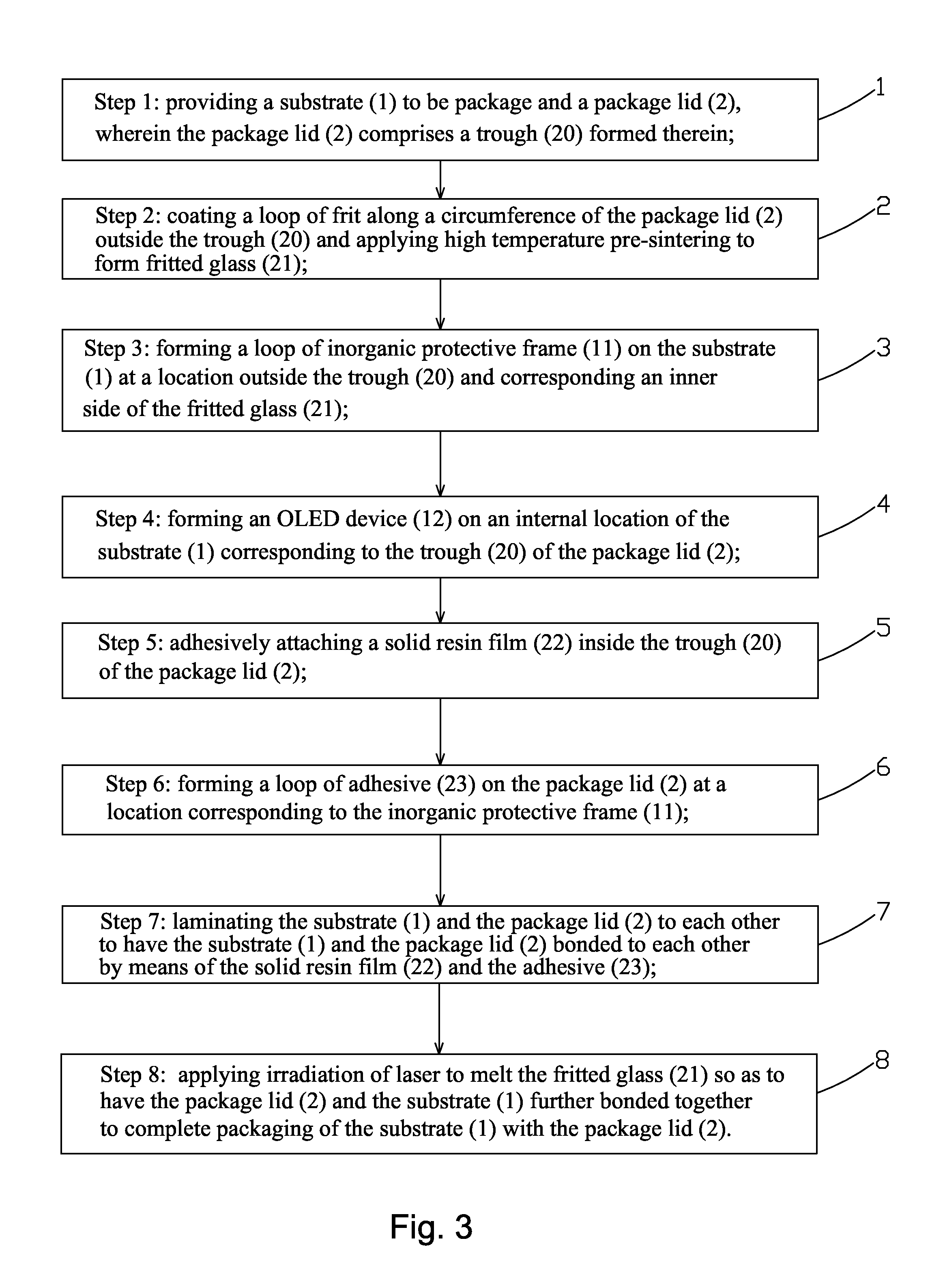
[0047]To further expound the technical solution adopted in the present invention and the advantages thereof, a detailed description is given to a preferred embodiment of the present invention and the attached drawings.

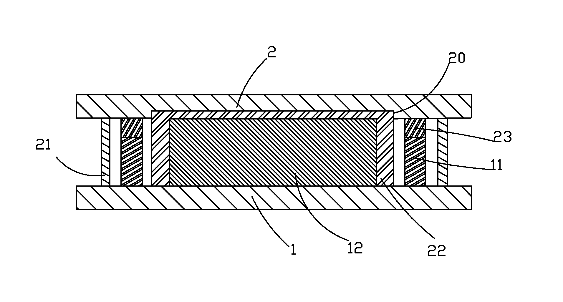
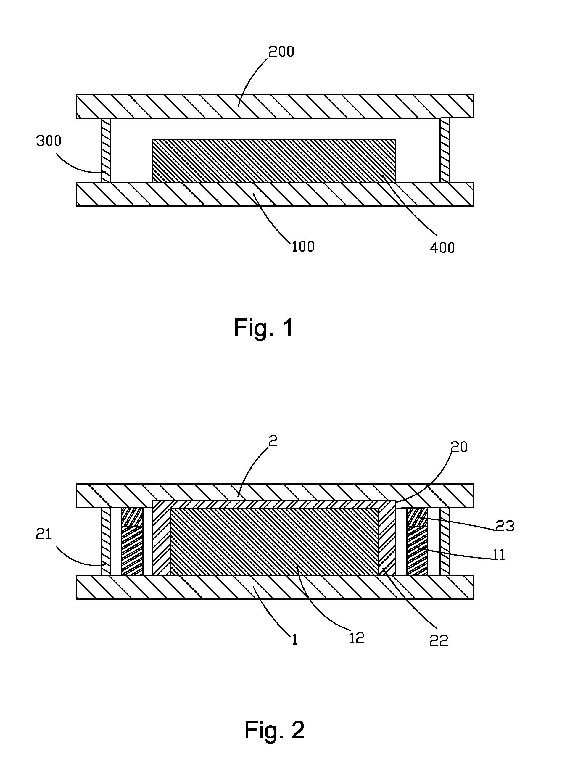
[0048]Referring to FIG. 2, the present invention provides an organic light-emitting diode (OLED) package structure, which comprises a substrate 1, a package lid 2 opposite to the substrate 1, an OLED device 12 located between the substrate 1 and the package lid2 and mounted on the substrate 1, a solid resin film 22 located between the substrate 1 and the package lid 2 and arranged on the package lid 2 to completely cover the OLED device 12, an inorganic protective frame 11 arranged on the substrate 1 and located outside an outer circumference of the solid resin film 22, adhesive 23 applied on the package lid 2 to bond the inorganic protective frame 11 and the package lid 2 to each other, and fritted glass 21 arranged outside an outer circumference of the inorganic prot...


PUM


Abstract

The present invention provides an OLED package structure and a packaging method. The structure includes a substrate (1), a package lid (2) opposite to the substrate (1), an OLED device (12) located between the substrate (1) and the package lid (2) and mounted on the substrate (1), a solid resin film (22) located between the substrate (1) and the package lid (2) and arranged on the package lid (2) to completely cover the OLED device (12), an inorganic protective frame (11) arranged on the substrate (1) and located outside an outer circumference of the solid resin film (22), adhesive (23) applied on the package lid (2) to bond the inorganic protective frame (11) and the package lid (2) to each other, and fritted glass (21) arranged outside an outer circumference of the inorganic protective frame (11) to bond the substrate (1) and the package lid (2) to each other. The present invention provides an arrangement where the inorganic protective frame is arranged inboard the fritted glass to effectively strengthen air tightness achieved with the fritted glass. Further, the solid resin film is arranged on the package lid to cover the OLED device so as to further strengthen the capability of the OLED package structure for blocking moisture and also, a gap in the interior of the sealed object is lessened so as to provide a sufficient mechanical strength to extend the lifespan of the OLED device.

Description

BACKGROUND OF THE INVENTION[0001]1. Field of the Invention[0002]The present invention relates to the field of packaging technology, and in particular to an OLED (Organic Light-Emitting Diode) package structure and a packaging method.[0003]2. The Related Arts[0004]OLED stands for organic light emitting diode, which has various advantages, such as being self-luminous, high brightness, wide view angle, high contrast, being flexible, and low power consumption and is considered the new generation of display measures that gradually takes the place of the conventional liquid crystal displays by being widely used in mobile phone screens, computer displays, and full-color televisions. The OLED displaying technology is different from the liquid crystal displaying technology in that no backlighting is needed and an extremely thin coating layer of an organic material and a glass substrate are used in such a way that when an electrical current flows therethrough, the organic material emits light...

Claims


Application Information

Patent Timeline
IPC IPC(8): H01L51/52H01L27/32H01L51/56
CPCH01L51/5246H01L51/56H01L2227/323H01L51/5253H01L27/3244H10K50/8426H10K50/844H10K59/12H10K71/00H10K59/1201
Inventor QIAN, JIAJIAWANG, YIFAN
Owner SHENZHEN CHINA STAR OPTOELECTRONICS TECH CO LTD
Why Eureka
Try Eureka