OLED backplate structure
a backplate and oled technology, applied in the field of display technology, can solve problems such as uneven brightness, and achieve the effects of improving uniformity, reducing cathode electrical resistance, and strong conductivity
- Summary
- Abstract
- Description
- Claims
- Application Information
AI Technical Summary
Benefits of technology
Problems solved by technology
Method used
Image
Examples
first embodiment
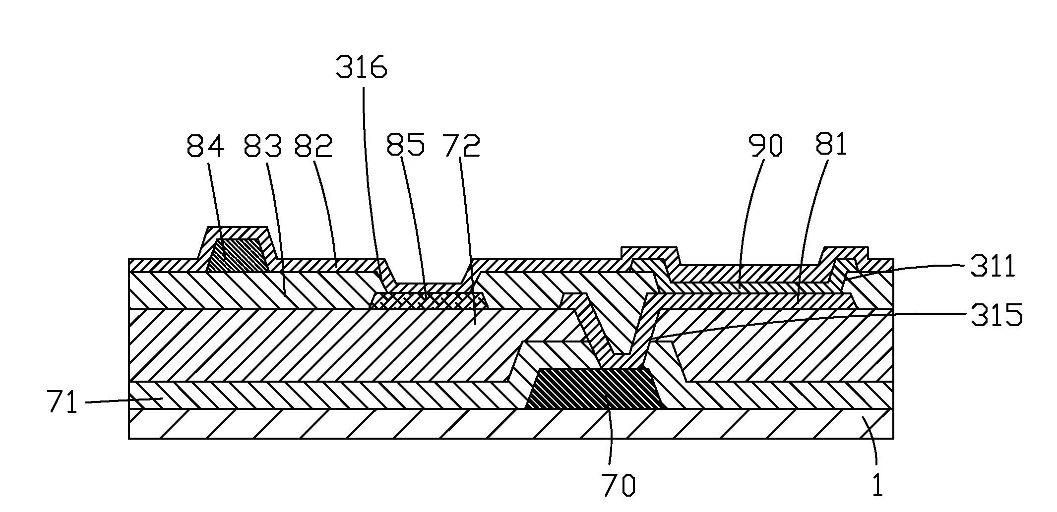
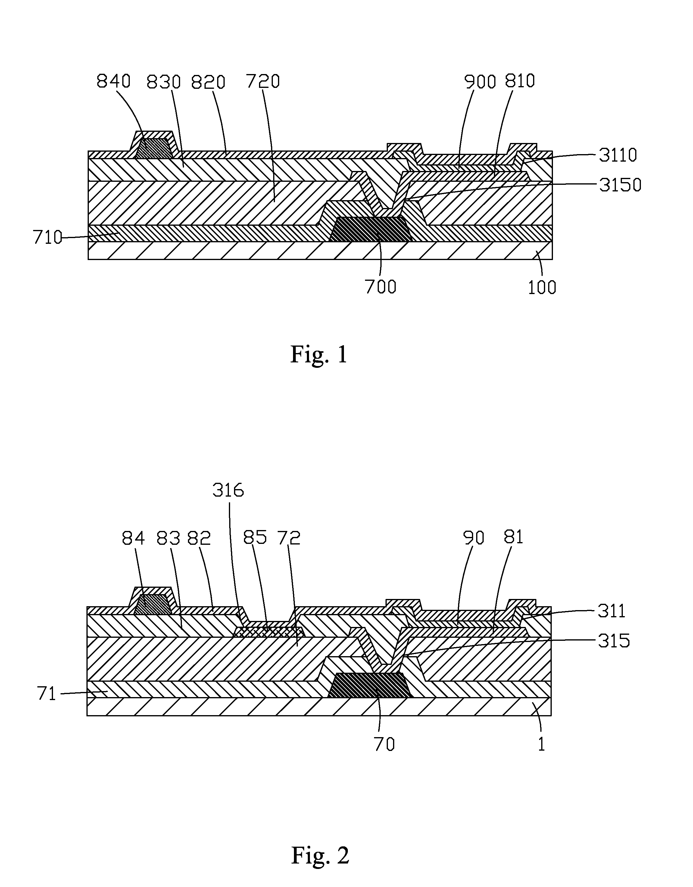
[0042]Please refer to FIG. 2 which is a sectional diagram of an OLED backplate structure according to the present invention. An auxiliary conducting layer 85 is provided on the second isolation layer 72, and the pixel definition layer 83 is provided with a third via 316 correspondingly above the auxiliary conducting layer 85, and the second electrode 82 contacts the auxiliary conducting layer 85 through the third via 316.
[0043]Specifically, the auxiliary conducting layer 85 and the first electrode 81 can be manufactured by employing the same mask.
[0044]Specifically, material of the auxiliary conducting layer 85 can be ITO or other conductive materials.
second embodiment
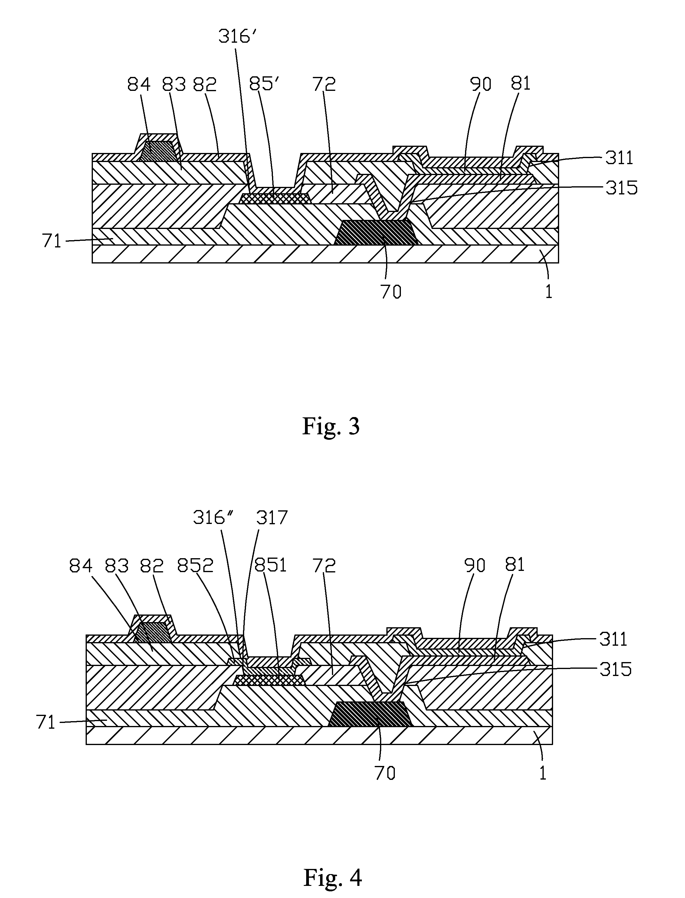
[0045]Please refer to FIG. 3, which is a sectional diagram of an OLED backplate structure according to the present invention. An auxiliary conducting layer 85′ is provided on the first isolation layer 71, and the pixel definition layer 83 and the second isolation layer 72 are provided with a third via 316′ correspondingly above the auxiliary conducting layer 85′, and the second electrode 82 contacts the auxiliary conducting layer 85′ through the third via 316′.
[0046]Specifically, the auxiliary conducting layer 85′ can be manufactured alone or manufactured with other conductive electrodes, such as the source / the drain of the TFT layer 70 at the same time.
[0047]Specifically, material of the auxiliary conducting layer 85′ can be ITO or other conductive materials.
third embodiment
[0048]Please refer to FIG. 4, which is a sectional diagram of an OLED backplate structure according to the present invention. The first isolation layer 71 is provided with a first auxiliary conducting layer 851, and the second isolation layer 72 is provided with a second auxiliary conducting layer 852, and the pixel definition layer 83 is provided with a third via 316″ correspondingly above the second auxiliary conducting layer 852, and the second isolation layer 72 is provided with a fourth via 317 correspondingly above the first auxiliary conducting layer 851; the second auxiliary conducting layer 852 contacts the first auxiliary conducting layer 851 through the fourth via 317, and the second electrode 82 contacts the second auxiliary conducting layer 852 through the third via 316″.
[0049]Specifically, material of the first auxiliary conducting layer 851 and the second auxiliary conducting layer 852 can be ITO or other conductive materials.
[0050]Significantly, in the aforesaid firs...
PUM
 Abstract
Description
Claims
Application Information
 - R&D Engineer
- R&D Manager
- IP Professional
- Industry Leading Data Capabilities
- Powerful AI technology
- Patent DNA Extraction
Browse by: Latest US Patents, China's latest patents, Technical Efficacy Thesaurus, Application Domain, Technology Topic, Popular Technical Reports.
© 2024 PatSnap. All rights reserved.Legal|Privacy policy|Modern Slavery Act Transparency Statement|Sitemap|About US| Contact US: help@patsnap.com


