Liquid Crystal Display Device and Method of Manufacturing the Same

a liquid crystal display and liquid crystal technology, applied in the field of display technology, can solve the problems of slow response speed of liquid crystal, limited viewing angle of liquid crystal display device, and possible dark-state light leakage, so as to reduce dark-state light leakage, reduce scattering phenomenon, and improve contrast

Inactive Publication Date: 2016-12-15
BOE TECH GRP CO LTD +1
View PDF10 Cites 5 Cited by
  • Summary
  • Abstract
  • Description
  • Claims
  • Application Information

AI Technical Summary

Benefits of technology

[0025]In the LCD device and the method of manufacturing the device according to the present invention, a nematic liquid crystal layer is disposed between the first substrate and the second substrate, wherein the nematic liquid crystal layer comprises a nematic liquid crystal and a polymer network, and wherein the polymer network is formed by irradiation polymerization of a functional monomer in a nematic liquid crystal mixture. The polymer network can reduce the scattering phenomena caused by the refractive index mismatch between liquid crystal and polymer in the prior LCD devices and significantly reduce the dark-state light leakage, so that the contrast is improved. Moreover, since there is no polymer projection disposed on the alignment layer according to the present invention, the dark-state light leakage caused by polymer projections is avoided and thus the contrast is further improved.

Problems solved by technology

However, the LCD devices also have shortcomings of limited viewing angle and slow response speed of liquid crystal.
However, dark-state light leakage may be caused by the refractive index mismatch between the liquid crystal and the polymer, as well as by the alignment difference between the areas around the polymer projections and the areas free of the polymer projections.

Method used


Image

  • Liquid Crystal Display Device and Method of Manufacturing the Same
  • Liquid Crystal Display Device and Method of Manufacturing the Same
  • Liquid Crystal Display Device and Method of Manufacturing the Same

Examples


Embodiment Construction

[0030]To enable a person skilled in the art to better understand the technical solution of the present invention, the LCD device and its manufacturing method according to the invention will be further described in detail with reference to the drawings.

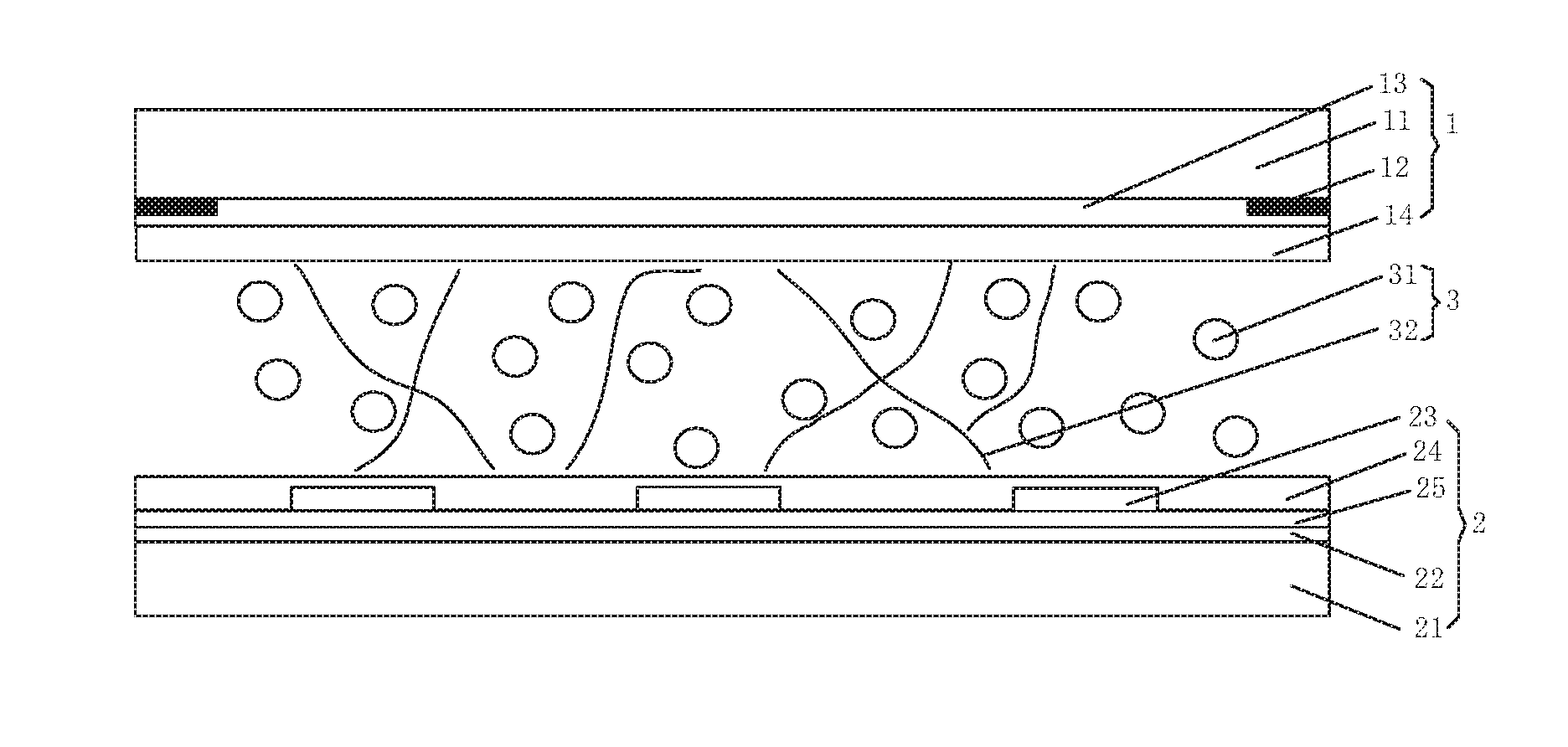
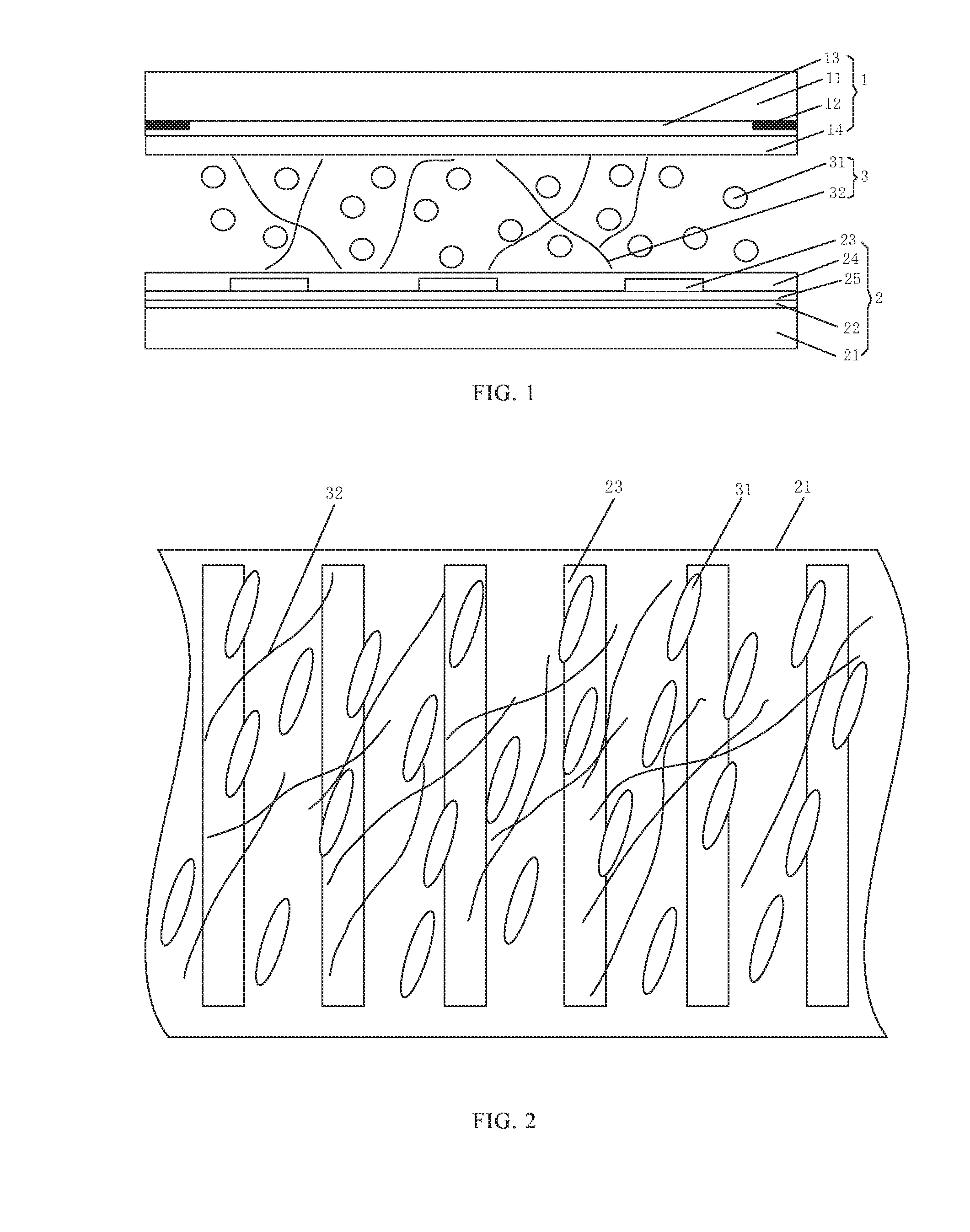
[0031]FIG. 1 is a schematic structure diagram of a LCD device according to an exemplary embodiment of the present invention, and FIG. 2 is a schematic plan view of the nematic liquid crystal layer of FIG. 1. As shown in FIGS. 1 and 2, the LCD device comprises a first substrate 1 and a second substrate 2 opposing each other, and a nematic liquid crystal layer 3 disposed between the first substrate 1 and the second substrate 2, wherein the nematic liquid crystal layer 3 comprises a nematic crystal 31 and a polymer network 32.

[0032]The LCD device of this exemplary embodiment is an ADS LCD device. The first substrate 1 is a color filter substrate, and the second substrate 2 is an array substrate. Specifically, the first substrate 1 may com...


PUM

PropertyMeasurementUnit
chemicalaaaaaaaaaa
photosensitiveaaaaaaaaaa
concentrationaaaaaaaaaa

Abstract

This invention discloses a liquid crystal display (LCD) device and a method of manufacturing the same. The LCD device comprises a first substrate and a second substrate opposing each other, and a nematic liquid crystal layer disposed therebetween and comprising a nematic liquid crystal and a polymer network. The polymer network is formed by irradiation polymerization of a functional monomer in a nematic liquid crystal mixture. The polymer network can reduce the scattering phenomena caused by the refractive index mismatch between liquid crystal and polymer in the prior LCD devices and significantly reduce the dark-state light leakage, so that the contrast is improved. Moreover, since there is no polymer projection disposed on the alignment layer according to the invention, the dark-state light leakage caused by polymer projections is avoided and thus the contrast is further improved.

Description

TECHNICAL FIELD[0001]This invention relates to the field of display technology, and particularly, to a liquid crystal display device and a method of manufacturing the same.BACKGROUND ART[0002]Currently, liquid crystal display (LCD) devices are widely used in displays, smart phones, televisions and other commercial products due to the advantages of low power consumption, light weight and thin thickness. However, the LCD devices also have shortcomings of limited viewing angle and slow response speed of liquid crystal. In order to overcome the above problems existed in the LCD devices, multi-domain vertical alignment technology or polymer-stabilized alignment technology is usually adopted in the LCD devices of the prior art, such that the LCD devices with broad viewing angle can be achieved and the response speed of liquid crystal in the LCD devices can be increased.[0003]Typically, polymer projections are formed on alignment layers of the LCD devices. The polymer projections can allow...

Claims


Application Information

Patent Timeline
Patent Type & Authority Applications(United States)
IPC IPC(8): G02F1/1334C09K19/54G02F1/1341
CPCG02F1/1334G02F1/1341C09K2019/546G02F2001/13345C09K19/542C09K19/38G02F1/133365G02F1/133707G02F1/13345C09K19/20C09K2019/0448C09K2019/2078G02F1/137G02F1/13775
Inventor ZHOU, XIAOCHENYANG, DENGKEQIN, GUANGKUI
Owner BOE TECH GRP CO LTD
Why Eureka
Try Eureka