Organic light emitting diode display apparatus

a light-emitting diode and display device technology, applied in the field of organic light-emitting diode display devices, can solve the problems of high resistance of light-emitting diodes, organic light-emitting diodes are vulnerable to moisture and/or gas, and light-emitting diodes can suffer from delamination, etc., to achieve excellent transparency, improve reliability in elapsed time, and secure reliability

Active Publication Date: 2016-12-22
SAMSUNG SDI CO LTD
View PDF2 Cites 1 Cited by
  • Summary
  • Abstract
  • Description
  • Claims
  • Application Information

AI Technical Summary

Benefits of technology

[0017]The present invention provides an organic light emitting diode display apparatus that includes an organic layer exhibiting excellent transparency.
[0018]The present invention provides an organic light emitting diode display apparatus that includes an organic layer capable of securing reliability in elapsed time by protecting the organic light emitting diode display apparatus from surroundings including moisture and gas.
[0019]The present invention provides an organic light emitting diode display apparatus, in which an organic layer more vulnerable to moisture and / or oxygen than an inorganic layer is formed so as not to be exposed at an edge of an encapsulation layer, thereby improving reliability in elapsed time.
[0020]The present invention provides an organic light emitting diode display apparatus, in which two adjacent inorganic layers are formed to contact each other to prevent slight lifting and / or delamination between the inorganic layers or between a substrate and an inorganic layer, thereby suppressing permeation of moisture and / or oxygen into an encapsulation layer through an edge thereof.

Problems solved by technology

Organic light emitting diodes are vulnerable to moisture and / or gas.
Organic light emitting diodes can suffer from delamination at an interface between a metal field and a light emitting layer due to moisture.
The organic light emitting diodes can have high resistance due to oxidation of metals and can suffer from degradation of organic materials in the light emitting layer due to moisture and / or oxygen.
The organic light emitting diode can suffer from deterioration in light emission due to oxidation of the light emitting layer or the metal field by outgassing inside or outside the organic light emitting diodes.
Etching of the organic layers can deteriorate an encapsulation function of the organic layers and provide adverse influence on formation of the inorganic layers.
If the organic layers exhibit low resistance to plasma, there can be difficulty in formation of the inorganic layers.
As a result, the organic light emitting diode can suffer from deterioration in luminous characteristics and reliability.
Thus, the encapsulation layer can suffer from slight lifting between the inorganic layers and / or delamination or slight lifting between the substrate and the inorganic layer.
As a result, the inorganic layers cannot sufficiently prevent moisture and / or oxygen from penetrating the organic light emitting diode.

Method used


Image

  • Organic light emitting diode display apparatus
  • Organic light emitting diode display apparatus
  • Organic light emitting diode display apparatus

Examples


example 2

Preparative Example 2

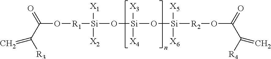
[0145]A monomer (molecular weight: 584.92 g / mol) represented by Formula 4 was prepared in the same manner as in Preparative Example 1 except that 21 g of 3,3-diphenyl-1,1,5,5-tetramethyltrisiloxane was used instead of 25 g of 3-phenyl-1,1,3,5,5-pentamethyltrisiloxane and 30.2 g of methacryloyl chloride was used instead of 34.3 g of acryloyl chloride. The obtained monomer had a purity of 96% as determined by HPLC. (1H NMR: δ7.52, m, 6H; δ7.42, m, 4H; δ6.25, d, 2H; δ6.02, dd, 2H; δ5.82, t, 1H; δ5.59, d, 2H; δ3.86, m, 4H; δ1.52, m, 4H; δ0.58, m, 4H; δ0.04, m, 12H)

example 3

Preparative Example 3

[0146]A monomer (molecular weight: 646.99 g / mol) represented by Formula 5 was prepared in the same manner as in Preparative Example 1 except that 21 g of 3,3-diphenyl-1,1,5,5-tetramethyltrisiloxane was used instead of 25 g of 3-phenyl-1,1,3,5,5-pentamethyltrisiloxane. The obtained monomer had a purity of 94% as determined by HPLC. (1H NMR: δ7.61, m, 6H; δ7.12, m, 4H; δ6.25, d, 2H; δ6.02, dd, 2H; δ5.82, t, 2H; δ3.87, m, 4H; δ1.54, m, 4H; δ0.58, m, 4H; δ0.02, m, 12H).

[0147]Details of components used in Examples and Comparative Examples were as follows.

[0148](A) Non-silicon-based di(meth)acrylate: (A1) 1,12-dodecanediol dimethacrylate (Sartomer Co., Ltd.), (A2) 1,10-decanediol dimethacrylate (Shin Nakamura Chemical Co., Ltd.).

[0149](B) Silicon-based di(meth)acrylate: (B1) monomer of Preparative Example 1, (B2) monomer of Preparative Example 2, (B3) monomer of Preparative Example 3.

[0150](C) Mono(meth)acrylate: (C1) HRI-07 (Daelim Chemical Co., Ltd.), (C2) benzyl me...

example 1

[0154]47.8 parts by weight of (A1), 28.7 parts by weight of (B1), 19.2 parts by weight of (C1) and 4.3 parts by weight of (D) were placed in a 125 ml brown polypropylene bottle, followed by mixing at room temperature for 3 hours using a shaker, thereby preparing an encapsulating composition (viscosity at 25° C.: 21 cPs).


PUM

PropertyMeasurementUnit
thicknessaaaaaaaaaa
heightaaaaaaaaaa
thicknessaaaaaaaaaa

Abstract

Disclosed is an organic light emitting diode display apparatus including: a substrate; an organic light emitting diode disposed on the substrate; and an encapsulation layer encapsulating the organic light emitting diode. The encapsulation layer has a structure in which two or more inorganic layers and one or more organic layers are alternately stacked one above another, two adjacent inorganic layers at least partially contact each other, and the organic layers are formed of an encapsulating composition. The encapsulating composition includes: about 10 wt % to about 70 wt % of (A) a non-silicon-based di(meth)acrylate, about 20 wt % to about 70 wt % of (B) a silicon-based di(meth)acrylate, about 5 wt % to about 40 wt % of (C) a mono(meth)acrylate, and about 1 wt % to about 10 wt % of (D) an initiator, the (B) silicon-based di(meth)acrylate being represented by Formula 1.

Description

CROSS-REFERENCE TO RELATED APPLICATION[0001]This application claims the benefit of Korean Patent Application No. 10-2015-0087823, filed on Jun. 19, 2015 in the Korean Intellectual Property Office, the entire disclosure of which is incorporated herein by reference.FIELD OF THE INVENTION[0002]The present invention relates to an organic light emitting diode display apparatus.DESCRIPTION OF THE RELATED ART[0003]Organic light emitting diodes are vulnerable to moisture and / or gas. Organic light emitting diodes can suffer from delamination at an interface between a metal field and a light emitting layer due to moisture. The organic light emitting diodes can have high resistance due to oxidation of metals and can suffer from degradation of organic materials in the light emitting layer due to moisture and / or oxygen. The organic light emitting diode can suffer from deterioration in light emission due to oxidation of the light emitting layer or the metal field by outgassing inside or outside t...

Claims


Application Information

Patent Timeline
Patent Type & Authority Applications(United States)
IPC IPC(8): H01L51/52H01L51/00
CPCH01L51/5256H01L51/0094H01L51/0043H01L2251/303H01L51/004H01L2251/558H10K59/12H10K50/844H10K50/8445
Inventor LEE, JI YEONNAM, SEONG RYONGKO, SUNG MINKIM, MI SUNKIM, HYE JINCHOI, MI JEONG
Owner SAMSUNG SDI CO LTD
Why Eureka
Try Eureka