Method for optical coating of large scale substrates

a technology of optical coating and substrate, applied in the direction of coatings, optical elements, instruments, etc., can solve the problems of large volume chambers for large astronomical mirrors, inapplicable coatings, and inability to achieve most uses in the optical thin-film industry. achieve the effect of shortening the duty cycl

Inactive Publication Date: 2016-12-29
RGT UNIV OF CALIFORNIA
View PDF10 Cites 3 Cited by
  • Summary
  • Abstract
  • Description
  • Claims
  • Application Information

AI Technical Summary

Benefits of technology

[0007]In contrast to prior methods, the present invention uses a novel technique employing Atomic Layer Deposition (ALD), a sequential form of Chemical Vapor Deposition (CVD), for depositing barrier / protection layers over the silver of large optical components. In contrast with conventional ALD techniques, the present provides techniques that use ALD with the substrate as a reaction chamber wall, matches the shape of the opposite wall to the substrate shape, or has a small reaction chamber height in order to keep the volume small and therefore keep duty cycles short.

Problems solved by technology

Conventional wisdom views ALD as not feasible to the coatings industry in general because it is inherently a slow process (only a few atomic layers per minute), whereas CVD and PVD can have the high deposition rates needed for mass production of parts.
This makes ALD impractical for most uses in the optical thin-film industry.
Very large astronomical mirrors, however, would require extremely large volume chambers using the conventional approach.
Moreover, the deposition process would be inefficient and very slow, due to the long times it would take to evacuate and purge such reaction chamber twice during each duty cycle.
PVD and other conventional coating techniques can have significant difficulties in achieving uniformity and precisely controlled layer thickness over large substrates.

Method used


Image

  • Method for optical coating of large scale substrates
  • Method for optical coating of large scale substrates
  • Method for optical coating of large scale substrates

Examples


Embodiment Construction

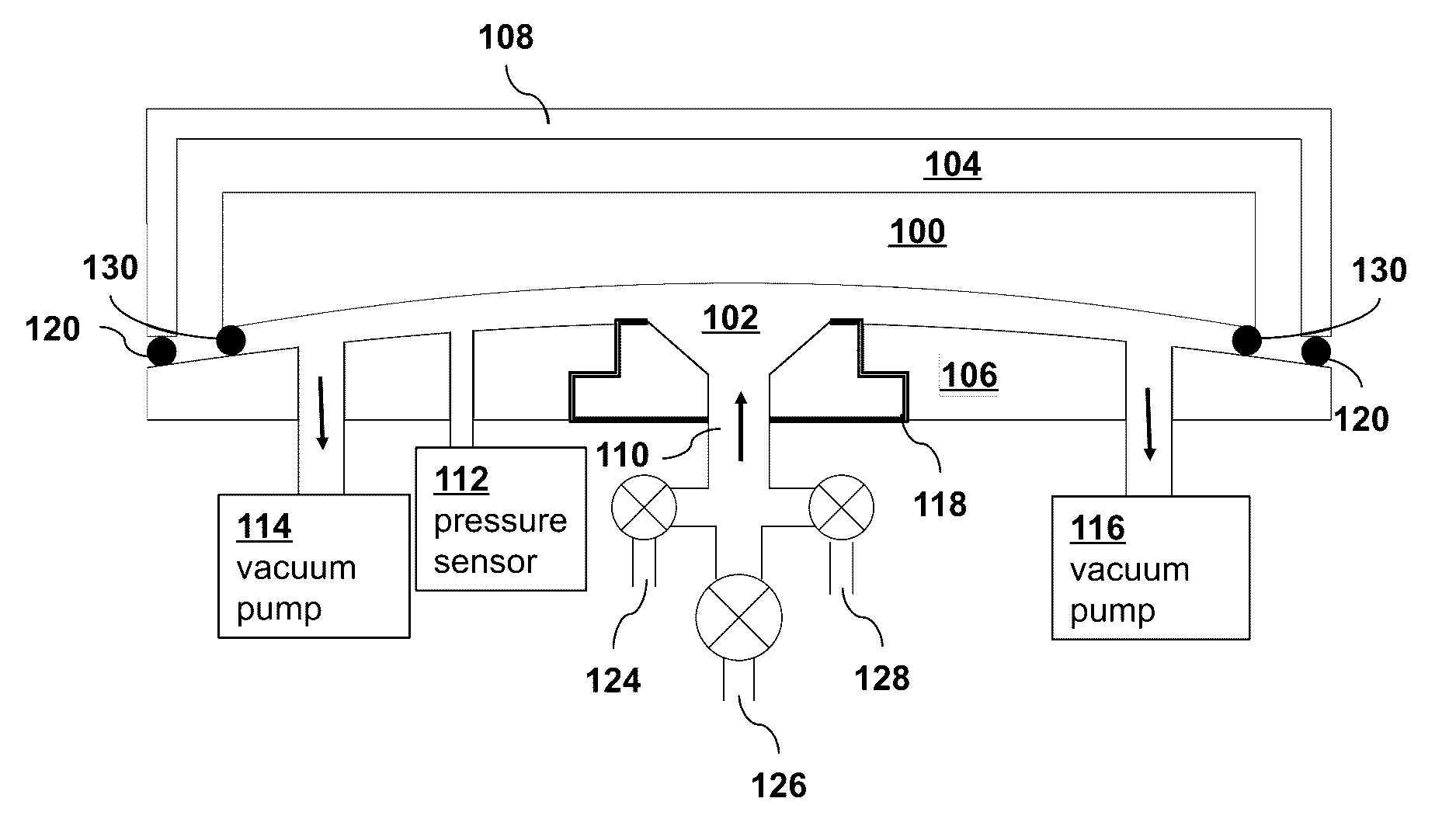
[0014]One embodiment of an apparatus for coating large substrates using ALD is shown in the schematic diagram of FIG. 1. A reaction chamber 102 is formed by joining a substrate 100 and a plate 106 using compliant seal 130.

[0015]The compliant seal is preferably an O-ring 130 that directly contacts an inside surface of the substrate 100 and an inside surface of the plate 106. The inside surface of the substrate 100 faces inside the reaction chamber 102 and an outside surface of the substrate faces outside the vacuum chamber 104. The outside surface typically includes a back surface and a side wall surface. The substrate thus forms one wall of the reaction chamber 102 and the plate 106 forms an opposite wall of the reaction chamber 102.

[0016]The inside surface of the plate 106 has a shape matching a shape of the inside surface of the substrate 100. In this context, matching shapes of the surfaces is defined to mean that the spacing between the surfaces is substantially uniform along th...


PUM

PropertyMeasurementUnit
ultraviolet wavelengthsaaaaaaaaaa
diameteraaaaaaaaaa
diameteraaaaaaaaaa

Abstract

A large substrate is optically coated in a reaction chamber that is formed by joining the substrate and a plate using a compliant seal, where the substrate forms one wall of the reaction chamber and the plate forms an opposite wall of the reaction chamber. The shape of the inside surface of the plate matches that of the inside surface of the substrate and they are spaced close together to minimize the volume of the reaction chamber. Atomic layer deposition is used to deposit one or more optical thin film layers to produce a coating on only the inside surface of the substrate. The outside surface is not coated.

Description

CROSS-REFERENCE TO RELATED APPLICATIONS[0001]This application claims priority from U.S. Provisional Patent Application 62 / 184,696 filed Jun. 25, 2015, which is incorporated herein by reference.STATEMENT OF GOVERNMENT SPONSORED SUPPORT[0002]This invention was made with Government support under contract NSF / AST1407353 awarded by the National Science Foundation. The Government has certain rights in the invention.FIELD OF THE INVENTION[0003]The present invention relates generally to methods and devices for depositing material coatings. More specifically, it relates to techniques for deposition of high quality optical coatings on very large substrates.BACKGROUND OF THE INVENTION[0004]Durable silver-based mirrors have long been a goal for astronomical telescopes. Silver is a relatively easy material to deposit and has excellent reflectivity and low emissivity in the visible and IR, but bare Ag quickly tarnishes (mostly due to oxidation with sulfur compounds) or forms salts with halides. T...

Claims


Application Information

Patent Timeline
Patent Type & Authority Applications(United States)
IPC IPC(8): C23C16/455
CPCC23C16/45525C23C16/4409C23C16/45504C23C16/45517C23C16/45555G02B5/10G02B1/10G02B1/11
Inventor PHILLIPS, ANDREW C.KOBAYASHI, NOBUHIKO
Owner RGT UNIV OF CALIFORNIA
Why Eureka
Try Eureka