Information processing device
- Summary
- Abstract
- Description
- Claims
- Application Information
AI Technical Summary
Benefits of technology
Problems solved by technology
Method used
Image
Examples
example 1
A. Configuration of Server
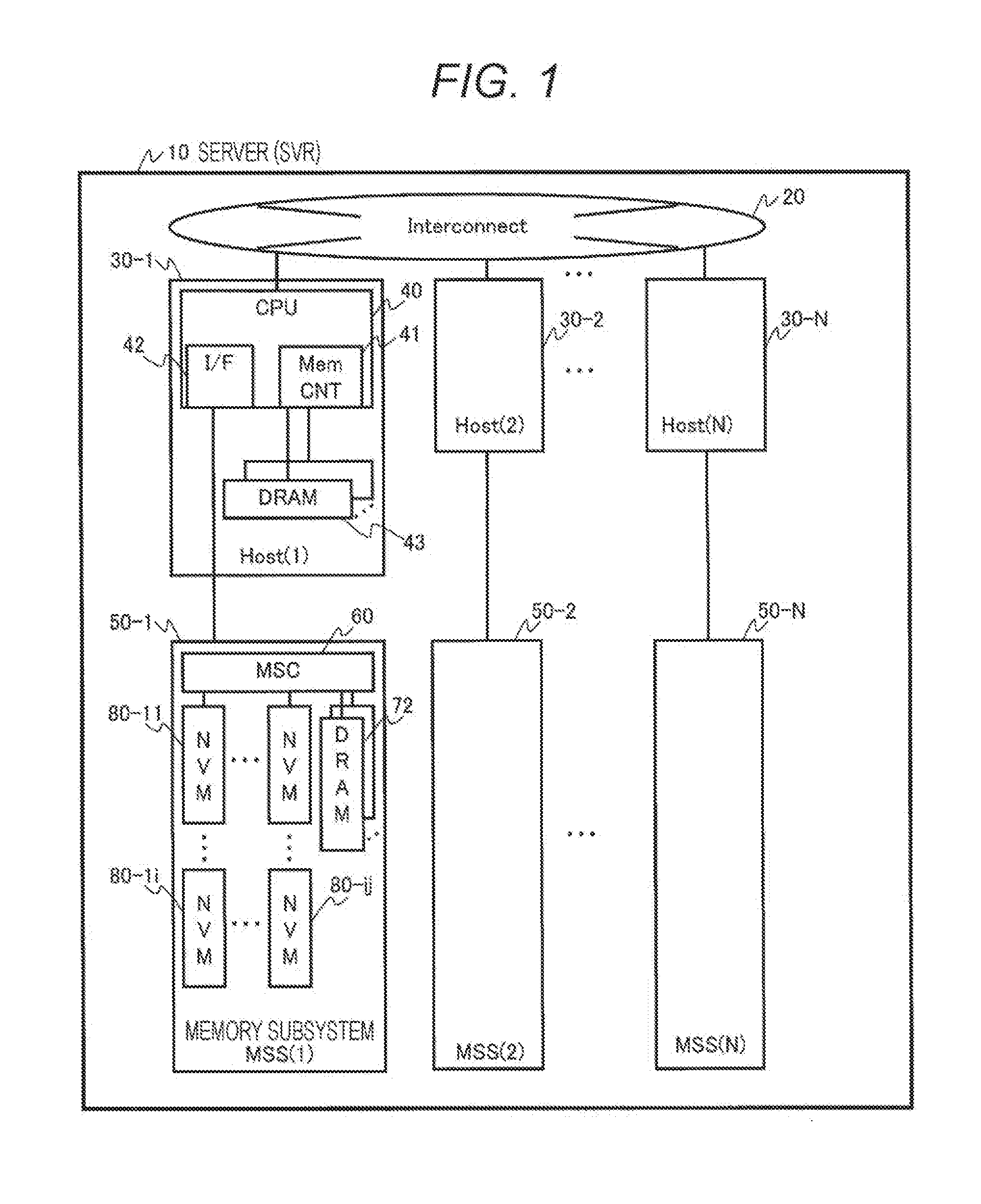
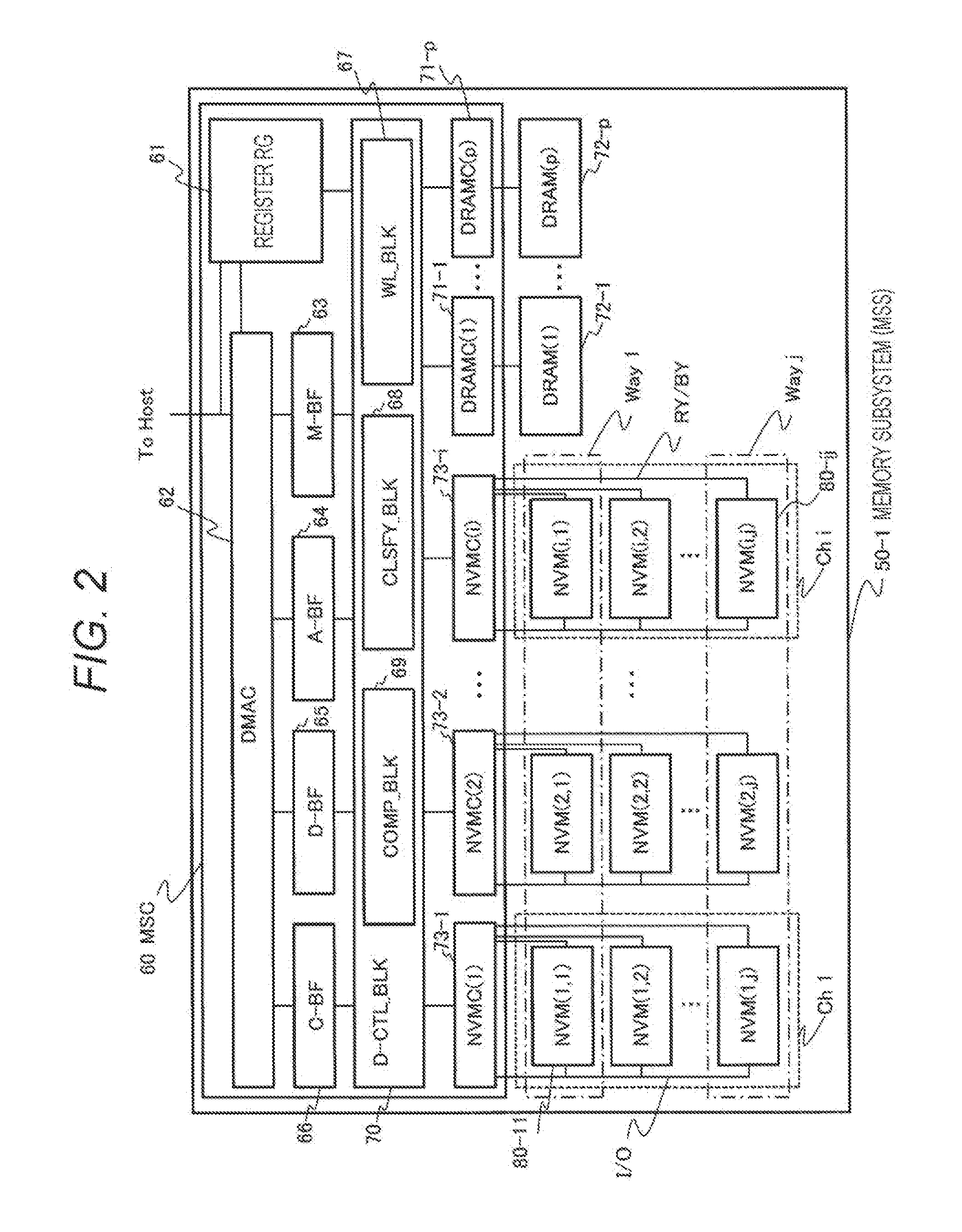
[0037]First, a configuration of a server (SVR) 10 will be described with FIGS. 1 and 2. FIG. 1 is a block diagram illustrating an overall configuration of the server (information processing apparatus) 10 to perform information processing.
[0038]The server (SVR) 10 includes a plurality of hosts (Host (1) 30-1 to Host (N) 30-N) to perform arithmetic processing, interconnect 20 connecting all of the hosts 30-1 to 30-N with each other, and a plurality of memory subsystems (MSS (1) to MSS (N)) 50-1 to 50-N connected to hosts 30-1 to 30-N thereof. Incidentally, the hosts 30-1 to 30-N are collectively denoted with a symbol 30 in the descriptions below. This similarly applies to other elements with a symbol without “-” collectively representing elements and a symbol added with “-” representing an individual element.
[0039]The host 30 includes an arithmetic module (CPU) 40 to perform arithmetic processing and one or more memories (DRAM) 43 connected to a memory contro...
example 2
[0120]The example 1 illustrates an example where the memory subsystem control module (MSC) 60 stores the data of the write request to the nonvolatile memory 80 in an uncompressed manner; however, the present example 2 illustrates an example of compressing data.
[0121]FIG. 11 is a block diagram illustrating exemplary correspondence relation among a chip, a block, and a page of a nonvolatile memory and a group of compressed data of the example 2. A DRAM 72 stores, in addition to the tables illustrated in the example 1, buffers 720-1 to 720-M for groups (1 to M), respectively, and a DRAM buffer management table 140. Other configurations are similar to those of the example 1 and thus overlapping descriptions thereon are omitted.
[0122]The buffers 720-1 to 720-M are storage areas to temporarily store compressed data by each of the groups 1 to M after a memory subsystem control module (MSC) 60 compresses data to write having received from a host 30.
[0123]The DRAM buffer management table 140...
example 3
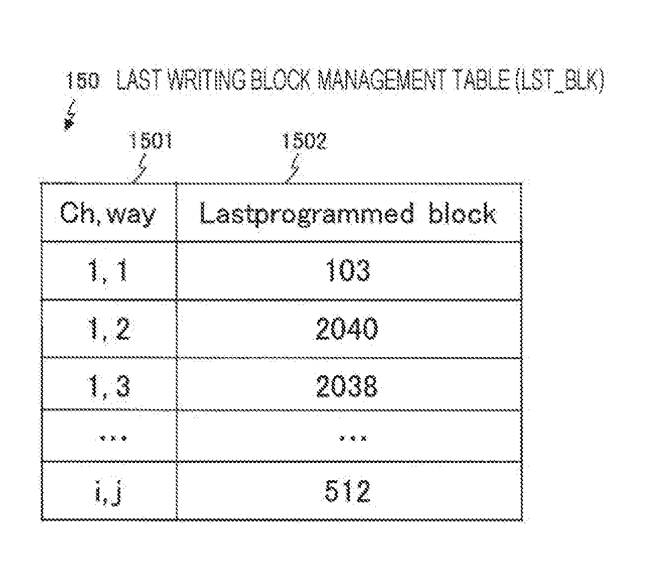
[0150]FIGS. 15 to 18 illustrate an example 3 where a last writing block management table 150 is added to the configuration of the example 1 and a writing destination is selected upon writing data to the memory subsystem 50.
[0151]First, overall processing will be described with FIG. 15. FIG. 15 is a block diagram illustrating exemplary correspondence relation among a chip and a block in a nonvolatile memory and a stored data type.
[0152]Together with a write request and data, a type of data (graph data (CSR), analysis result (MSG), vertex information (VAL), etc.) is notified from the host 30 to a memory subsystem control module (MSC) 60. The memory subsystem control module (MSC) 60 changes a method of selecting a writing destination of the data based on the type of the data received.
[0153]In the example where graph data (CSR) is not updated until termination of graph processing as illustrated in FIG. 5 of the example 1, the graph data is not updated during the graph processing but an ...
PUM
 Abstract
Description
Claims
Application Information


