

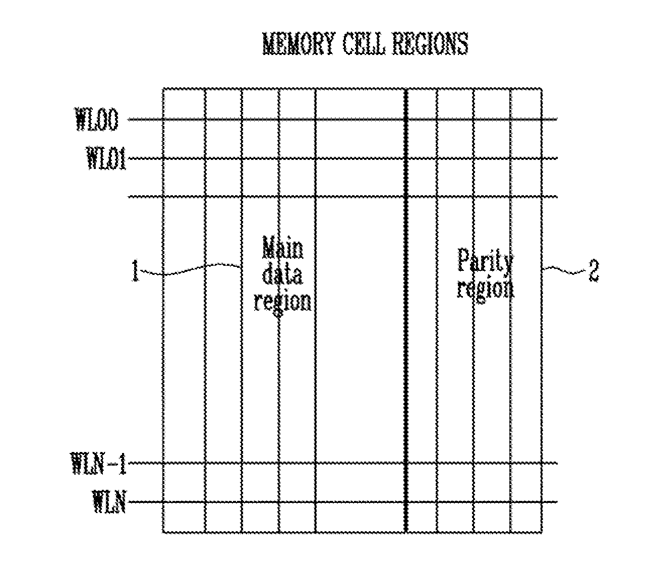
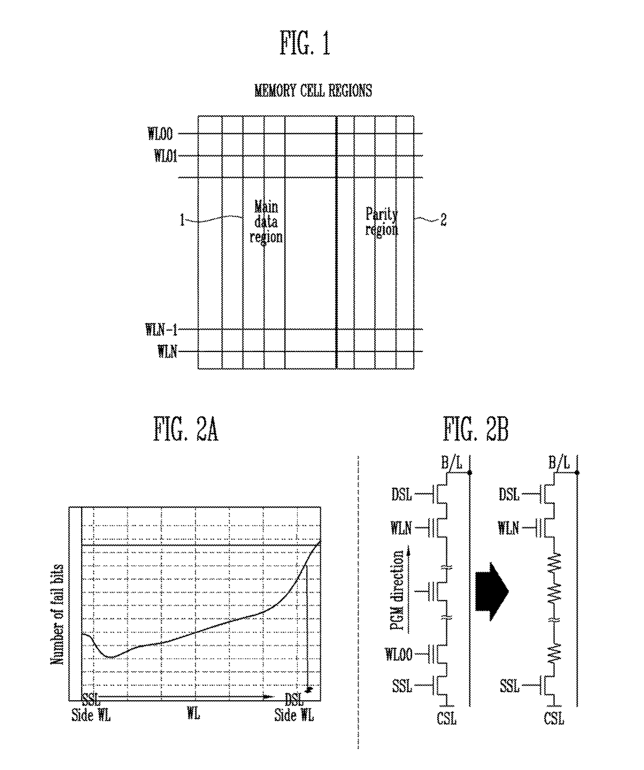
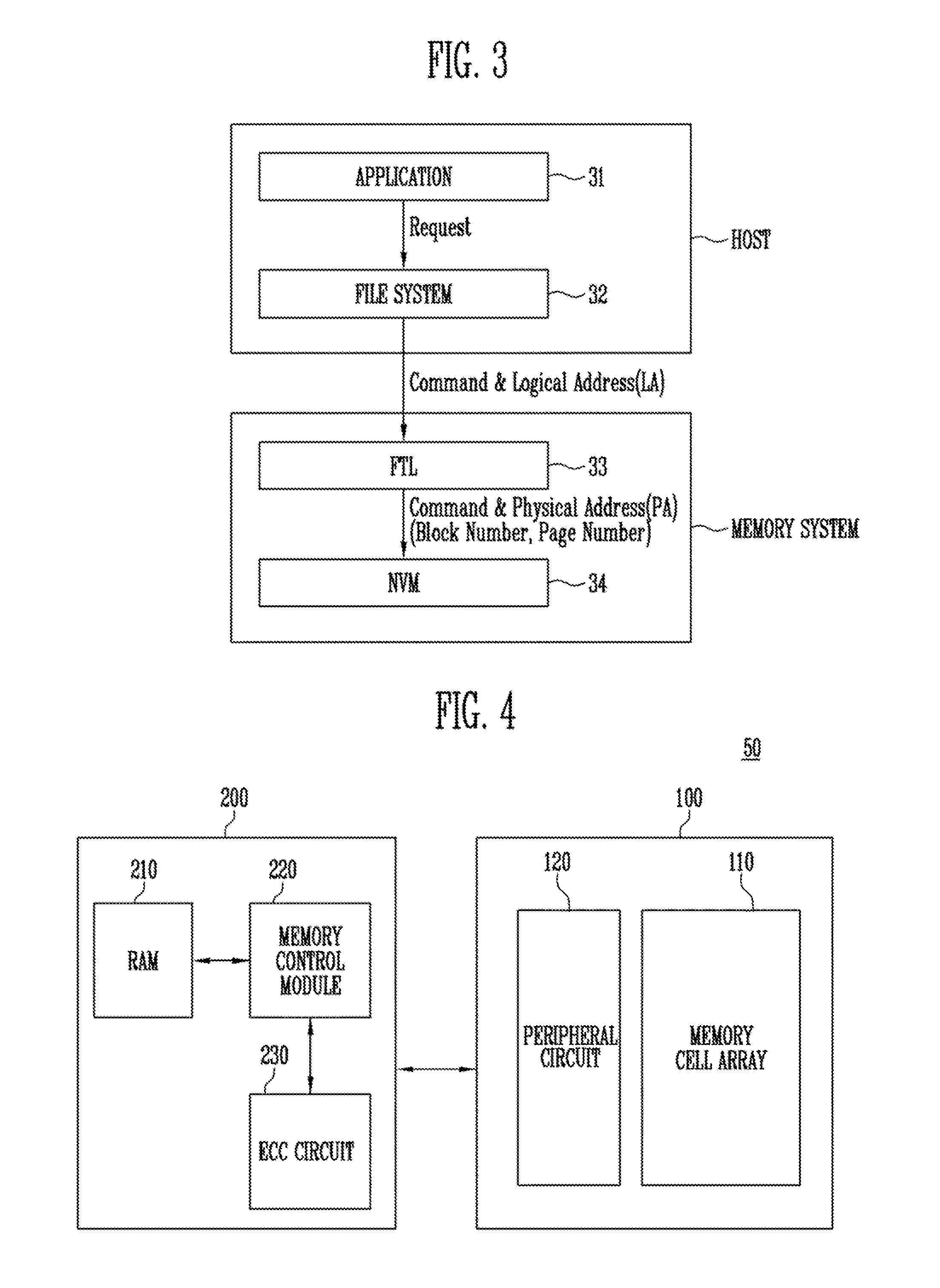
Memory device with different parity regions
a memory device and parity region technology, applied in the field of electronic devices, can solve problems such as loss of stored data in memory devices, and achieve the effect of improving error correction capacity and enhancing overall reliability of memory devices
- Summary
- Abstract
- Description
- Claims
- Application Information
AI Technical Summary
Benefits of technology
Problems solved by technology
Method used
Image

Examples
Embodiment Construction
[0038]Examples of various embodiments are illustrated in the accompanying drawings and described further below. It will be understood that the discussion herein is not intended to limit the claims to the specific embodiments described. On the contrary, it is intended to cover alternatives, modifications, and equivalents as may be included within the spirit and scope of the present disclosure as defined by the appended claims.
[0039]Example embodiments will be described in more detail with reference to the accompanying drawings. The present disclosure, however, may be embodied in various different forms, and should not be construed as being limited to only the illustrated embodiments herein. Rather, these embodiments are provided as examples so that this disclosure will be thorough and complete, and will fully convey the aspects and features of the present disclosure to those skilled in the art.
[0040]It will be understood that, although the terms “first”, “second”, “third”, and so on ...
PUM
 Abstract
Description
Claims
Application Information