Display device and method for driving same

a display device and display technology, applied in the field of display devices, can solve the problems of degrading display quality, high definition, and difficult to achieve large size, so as to minimize the occurrence of grayscale failures and extend the life of display devices

Active Publication Date: 2017-01-26
SHARP KK
View PDF2 Cites 51 Cited by
  • Summary
  • Abstract
  • Description
  • Claims
  • Application Information

AI Technical Summary

Benefits of technology

[0131]According to the first aspect of the present invention, with at least either one of the drive transistor and the electrooptical element serving as target circuit element, an amount of change in threshold voltage of the target circuit element is found, and the value of the low-level power supply voltage is adjusted depending on the amount of change. Hence, a grayscale voltage range (a range of data voltage required to perform desired grayscale display) can be shifted depending on the degree of change in the characteristic of the target circuit element. By this, the occurrence of a grayscale failure is prevented. In addition, since the occurrence of a grayscale failure is prevented, an effect of extending the life of the display device can also be obtained. By the above, a display device capable of compensating for changes in the characteristics of circuit elements without causing a grayscale failure is implemented.
[0132]According to the second aspect of the present invention, while a component for detecting characteristics of the circuit elements in the pixel circuits is utilized, the value of the low-level power supply voltage can be adjusted.
[0133]According to the third aspect of the present invention, a display device capable of compensating for degradation of circuit elements caused by the passage of time is implemented without causing a grayscale failure.
[0134]According to the fourth aspect of the present invention, an amount of change in threshold voltage is found based on a difference

Problems solved by technology

As for an organic EL display device employing the passive matrix system, its structure is simple, but a large size and high definition are difficult to achieve.
When the drive t

Method used


Image

  • Display device and method for driving same
  • Display device and method for driving same
  • Display device and method for driving same

Examples


Embodiment Construction

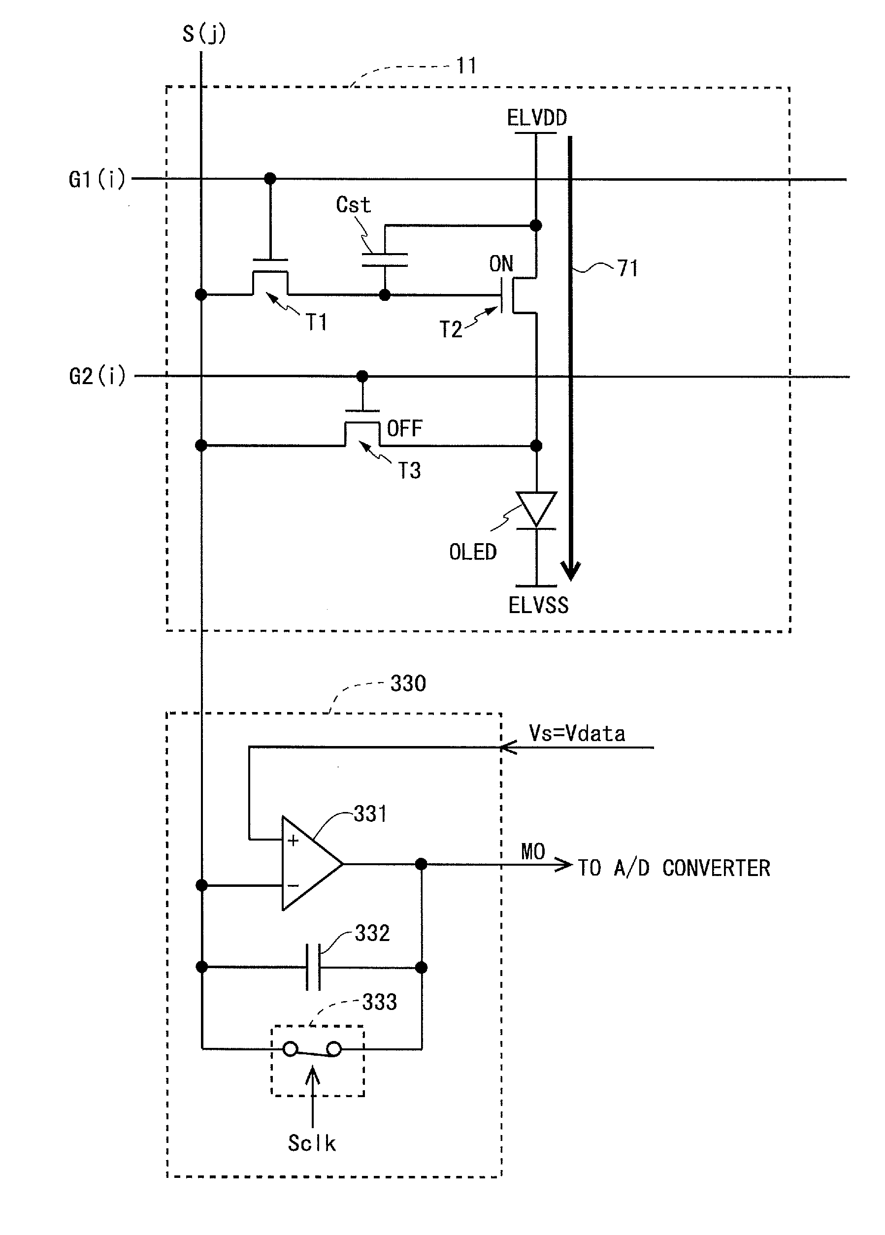
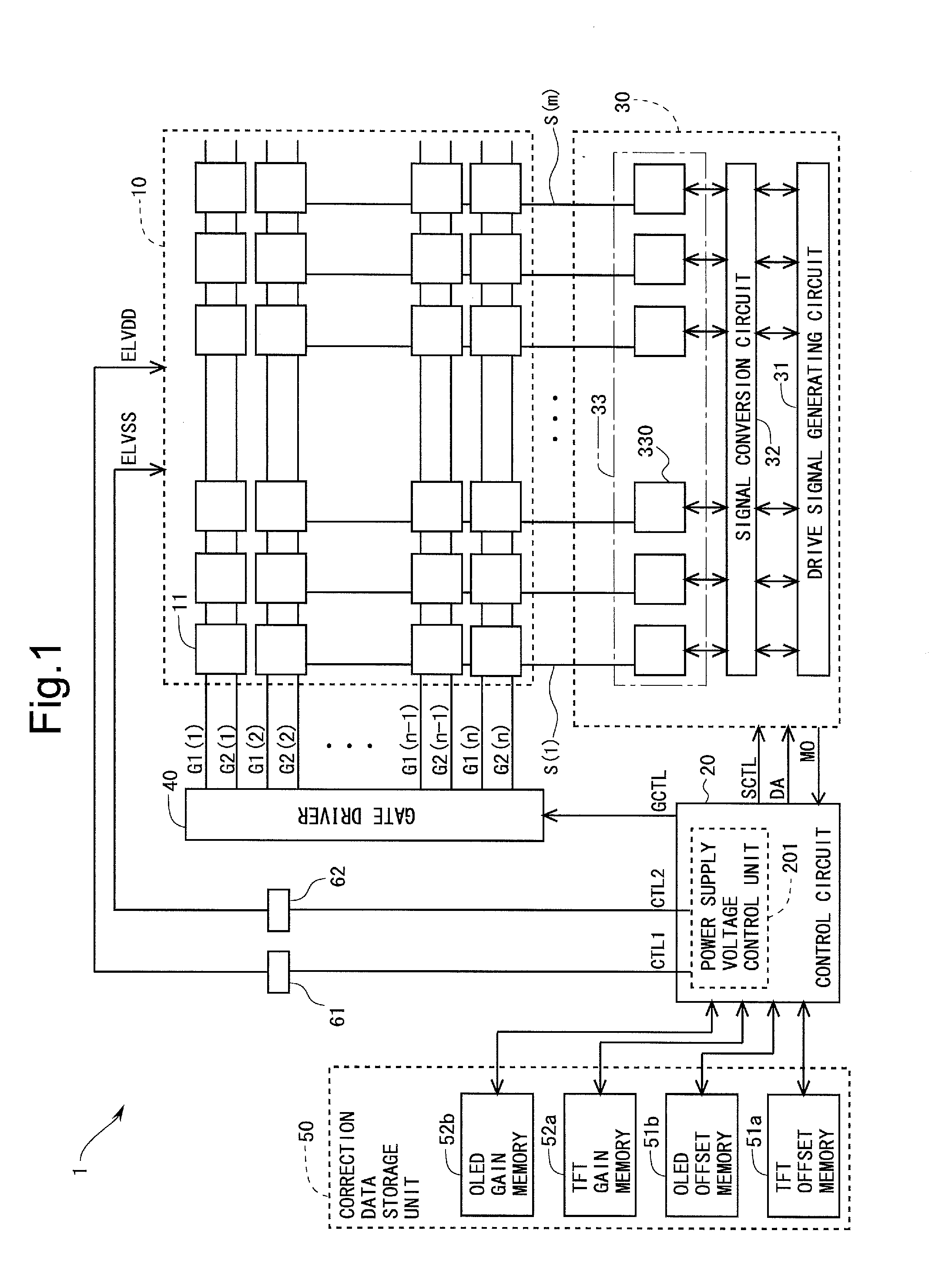
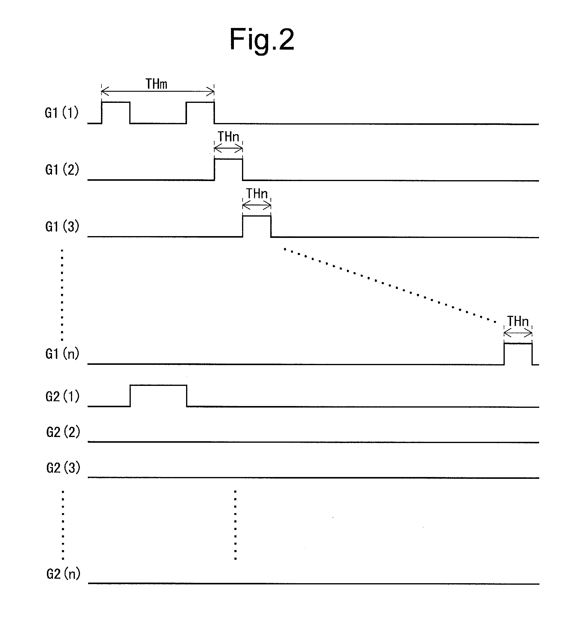
[0204]One embodiment of the present invention will be described below with reference to the accompanying drawings. Note that in the following it is assumed that m and n are integers greater than or equal to 2, i is an integer between 1 and n, inclusive, and j is an integer between 1 and m, inclusive. Note also that in the following the characteristics of a drive transistor provided in a pixel circuit are referred to as “TFT characteristics”, and the characteristics of an organic EL element provided in the pixel circuit are referred to as “OLED characteristics”.

[0205]

[0206]FIG. 1 is a block diagram showing an overall configuration of an active matrix-type organic EL display device 1 according to one embodiment of the present invention. The organic EL display device 1 includes a display unit 10, a control circuit 20, a source driver (data line drive circuit) 30, a gate driver (scanning line drive circuit) 40, correction data storage unit 50, an organic EL high-level power supply 61, a...


PUM


Abstract

Based on the results of detection of characteristics of drive transistors and organic EL elements, a control circuit finds magnitudes of threshold shifts of the drive transistors and the organic EL elements. A power supply voltage control unit sets a value of a low-level power supply voltage to a value lower, by a voltage value corresponding to an average value of the magnitudes of the threshold shifts for all pixels, than a value at an initial point in time. Furthermore, the power supply voltage control unit adjusts a value of a high-level power supply voltage, depending on magnitudes of mobilities obtained by detection of characteristics of the drive transistors.

Description

TECHNICAL FIELD[0001]The present invention relates to a display device and a method for driving the same, and more specifically to a display device provided with a pixel circuit including an electrooptical element such as an organic EL (Electro Luminescence) element, and a method for driving the same.BACKGROUND ART[0002]As a display element provided in a display device, there have hitherto been an electrooptical element whose luminance is controlled by an applied voltage, and an electrooptical element whose luminance is controlled by a flowing current. Examples of the electrooptical element whose luminance is controlled by an applied voltage include a liquid crystal display element. Meanwhile, examples of the electrooptical element whose luminance is controlled by a flowing current include an organic EL element. The organic EL element is also called an OLED (Organic Light-Emitting Diode). An organic EL display device that uses the organic EL element being a spontaneous electrooptica...

Claims


Application Information

Patent Timeline
IPC IPC(8): G09G3/3233G09G3/3291
CPCG09G2310/08G09G2300/0809G09G3/3233G09G2310/0289G09G2330/028G09G2320/0233G09G2320/046G09G3/3291
Inventor TAKIZAWA, KAZUOKISHI, NORITAKA
Owner SHARP KK
Why Eureka
Try Eureka