

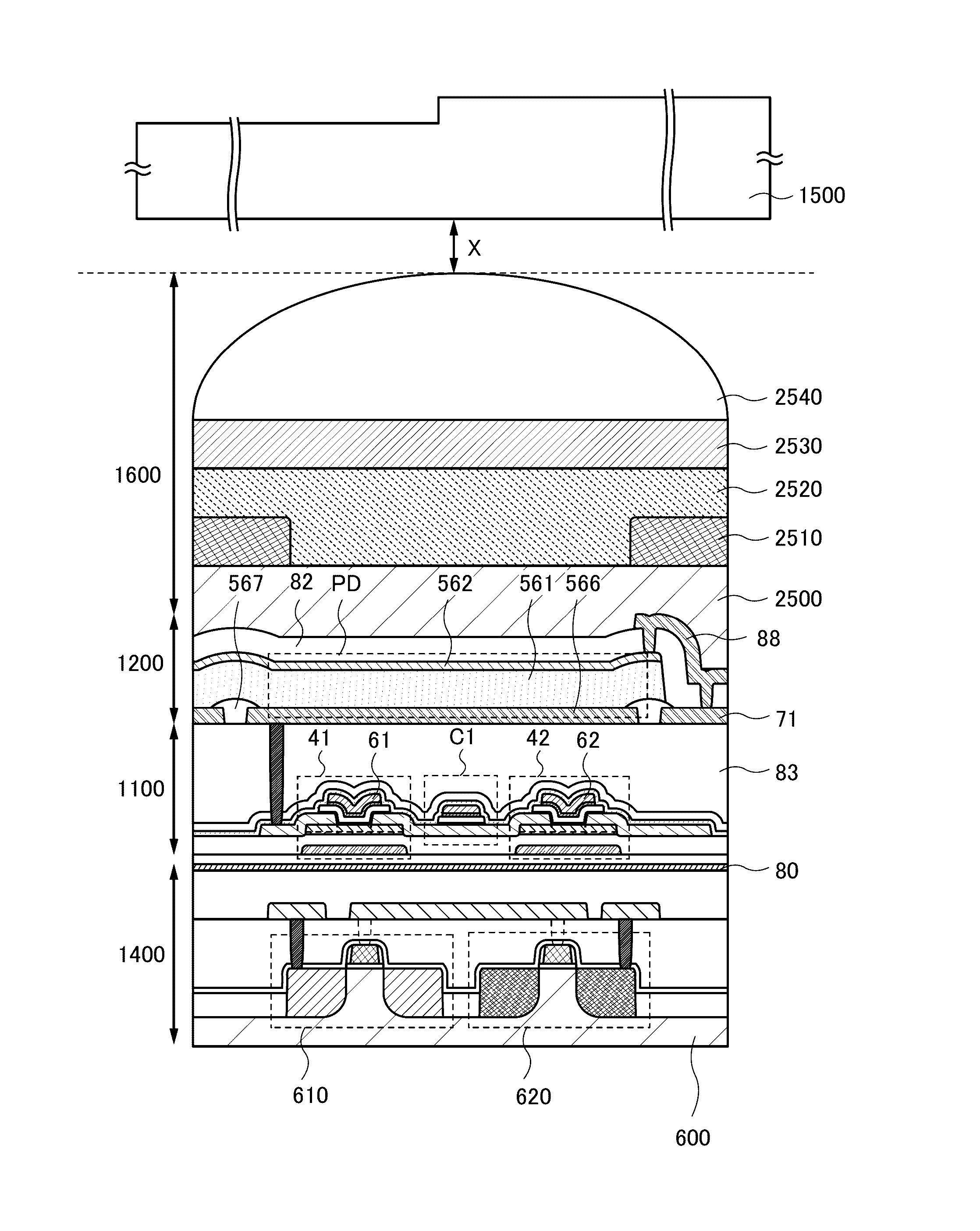
Imaging device and electronic device
a technology of electronic devices and imaging devices, applied in the direction of radio frequency controlled devices, transistors, television systems, etc., can solve the problems of increasing the difficulty of the transistor manufacturing process, difficult to suppress the variation in electrical characteristics, etc., and achieves low noise, high-quality imaging data, and low power consumption
- Summary
- Abstract
- Description
- Claims
- Application Information
AI Technical Summary
Benefits of technology
Problems solved by technology
Method used
Image

Examples
embodiment 1
[0098]In this embodiment, an imaging device that is one embodiment of the present invention is described with reference to drawings.
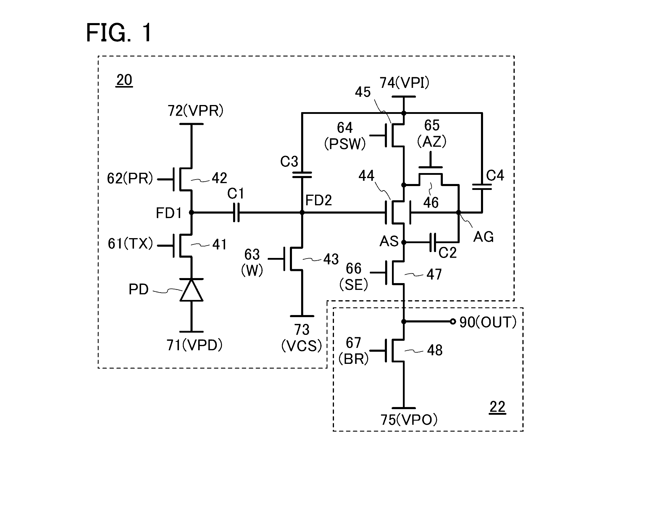
[0099]One embodiment of the present invention is a pixel circuit including a circuit for correcting variation in the threshold voltage of a transistor. The transistor includes two gates facing each other with a channel formation region provided therebetween. The transistor operates in such a manner that one of the gates holds a potential for correcting variation in the threshold voltage and the other thereof is supplied with a potential corresponding to imaging data. Therefore, high-quality imaging data with low noise can be obtained.
[0100]FIG. 1 is an example of a circuit diagram of a circuit 20 that can function as a pixel and a circuit 22 that can function as a current source circuit included in an imaging device in one embodiment of the present invention. Although an example in which n-channel transistors are used is illustrated in FIG. 1 and the li...
embodiment 2
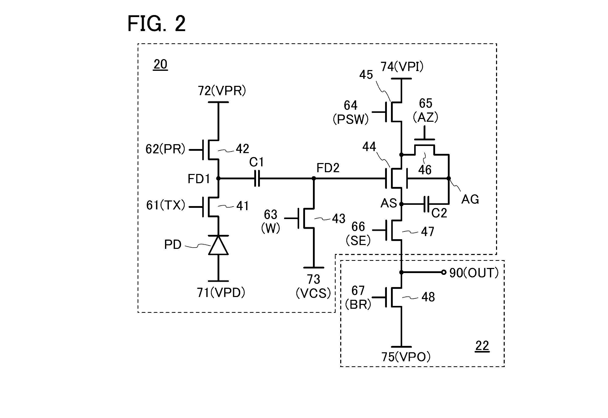
[0213]In this embodiment, an example of a driving method of a pixel circuit is described. The pixel circuit described in Embodiment 1 can perform first operation in which normal imaging is performed and second operation in which difference data between imaging data of an initial frame and imaging data of a current frame can be retained and a signal based on the difference data can be output. In the second operation, the difference data can be output without a comparison process or the like in an external circuit; thus, the power consumption of a security camera or the like can be reduced.
[0214]The first operation of the circuit in FIG. 1 is described with reference to a timing chart in FIG. 31. Note that a potential for correcting variation in the threshold voltage of the transistor 44 is held on the back gate side of the transistor 44 by the operation method described in Embodiment 1.
[0215]In a period from time T1 to time T2, the potential of the wiring 61 (TX) is set to “H”, the p...
embodiment 3
[0235]In this embodiment, a transistor including an oxide semiconductor that can be used in one embodiment of the present invention is described with reference to drawings. In the drawings in this embodiment, some components are enlarged, reduced in size, or omitted for easy understanding.
[0236]FIGS. 35A and 35B are a top view and a cross-sectional view illustrating a transistor 101 of one embodiment of the present invention. FIG. 35A is the top view, and FIG. 35B illustrates a cross section in the direction of dashed-dotted line B1-B2 in FIG. 35A. A cross section in the direction of dashed-dotted line B3-B4 in FIG. 35A is illustrated in FIG. 37A. The direction of dashed-dotted line B1-B2 is referred to as a channel length direction, and the direction of dashed-dotted line B3-B4 is referred to as a channel width direction.
[0237]The transistor 101 includes an insulating layer 120 in contact with a substrate 115; an oxide semiconductor layer 130 in contact with the insulating layer 12...
PUM
 Abstract
Description
Claims
Application Information