Optimized wavelength photon emission microscope for VLSI devices

a wavelength photon emission microscope and wavelength-dependent technology, applied in the field of photon emission microscopy, can solve the problems of inability to have a p-n junction forward-biased with more than 1-2 v, interference more with observations at these longer wavelengths, and very faint hc emission

Active Publication Date: 2017-02-23
FEI CO
View PDF4 Cites 0 Cited by
  • Summary
  • Abstract
  • Description
  • Claims
  • Application Information

AI Technical Summary

Benefits of technology

[0011]Some existing designs limit the range of observation to 1.5 um (which coincides with the sensitivity of InGaAs cameras) an

Problems solved by technology

In general, it is not possible to have a p-n junction forward-biased with more than 1-2 V due to the extremely high current densities that would be obtained.
For common VLSI devices, however, the HC emissions are very faint, and since the amount of noise originating in thermal emissions (which follows the black body radiation spectral distribution) increases with wavelength, it interferes more with observations at these longer wavelengths.
The faint HC emissions also cause the exposure times to be as long as hundreds of seconds, which

Method used


Image

  • Optimized wavelength photon emission microscope for VLSI devices
  • Optimized wavelength photon emission microscope for VLSI devices
  • Optimized wavelength photon emission microscope for VLSI devices

Examples


Embodiment Construction

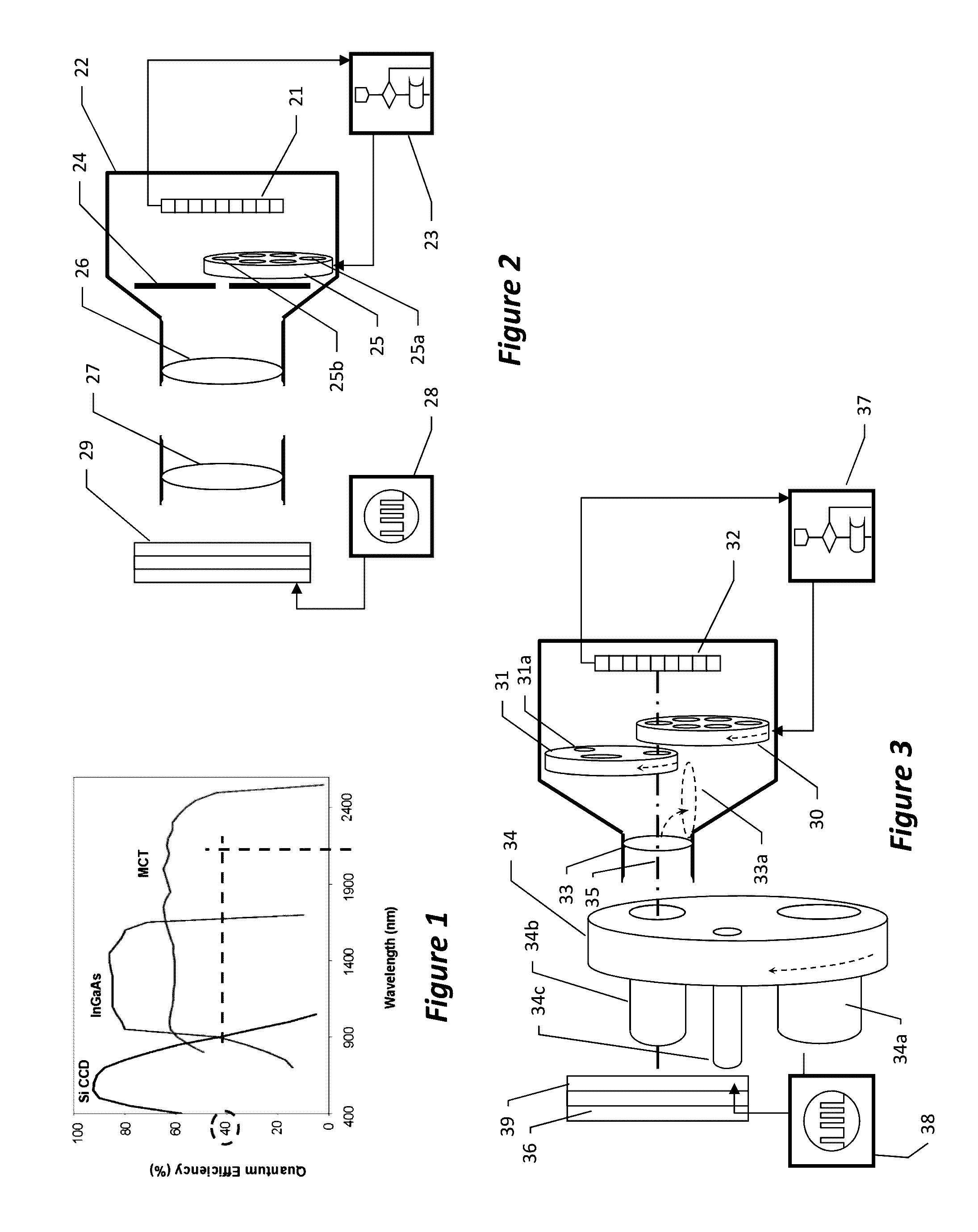
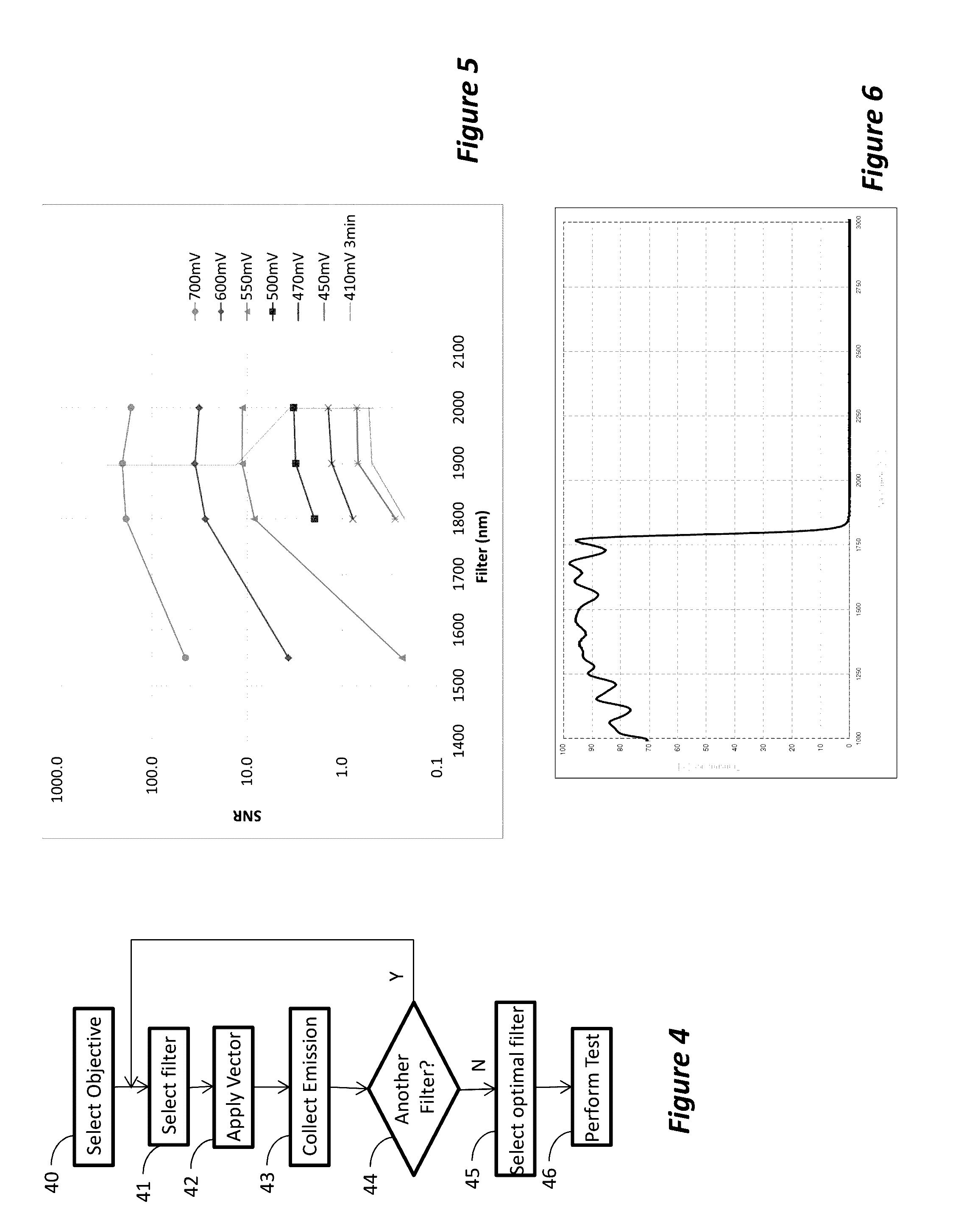
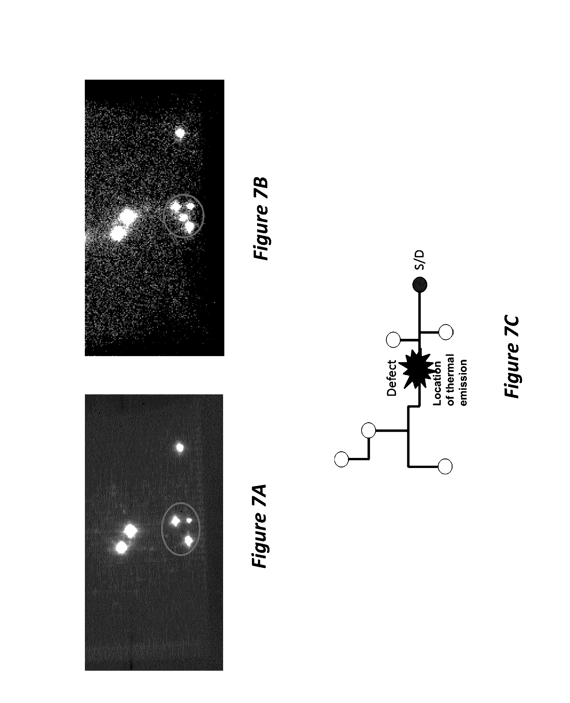
[0032]Described herein are methods for testing semiconductor chips (IC) for various faults. The testing is done while applying test signal to the IC and performing different types of imaging of the IC during the testing. The different images obtained are compared to identify faults. The methods employ the ability to insert and remove various filters in the optical path of the imaging system. It has been discovered by the inventor that certain faults can be identified by comparing images taken with and without the filters. It has also been discovered by the inventor that certain faults can be identified by comparing optical emission images with thermal images.

[0033]According to one example, test signals are applied to the IC, such that switching transistors emit photons. An emission filter, e.g., a band filter, that passes light with wavelength below 2000 nm or below 1600 nm (if the signal is strong enough), is used to obtain an emission image. This image will basically consist of “d...


PUM


Abstract

A method for emission testing of a semiconductor device (DUT), by mounting the DUT onto an test bench of an emission tester, the emission tester having an optical detector; electrically connecting the DUT to an electrical tester; applying electrical test signals to the DUT while keeping test parameters constant; inserting an optical filters into an optical path of the emission tester and collecting emission test signal from the optical detector; removing the filter from the optical path and collecting emission test signal from the optical detector. Comparing the images obtained with and without the filter. The filter may be shortpass to obtain emission signal, a bandpass for detecting forward bias, or longpass to obtain thermal signal.

Description

RELATED APPLICATIONS[0001]The present application claims priority benefit from U.S. Provisional Application No. 62 / 237,399, filed on Oct. 5, 2015. The present application is also a continuation-in-part of U.S. patent application Ser. No. 14 / 250,361, filed Apr. 10, 2014, which claims priority benefit from U.S. Provisional Application No. 61 / 810,645, filed on Apr. 10, 2013, the disclosures of all of which are incorporated herein in their entireties.GOVERNMENT LICENSE RIGHTS[0002]This invention is based upon work supported by the Office of the Director of National Intelligence (ODNI), Intelligence Advanced Research Projects Activity (IARPA), via Air Force Research Laboratory (AFRL) contract number FA8650-11-C-7105. The ideas and conclusions contained herein are those of the inventors and should not be interpreted as necessarily having the official endorsements, either expressed or implied, of ODNI, IARPA, AFRL, or the U.S. Government.FIELD[0003]The present application belongs to the fi...

Claims


Application Information

Patent Timeline
IPC IPC(8): G01R31/27G01R31/311
CPCG01R31/311G01R31/275G01R31/2656
Inventor DESLANDES, HERVE
Owner FEI CO
Why Eureka
Try Eureka