Pixel circuit
a pixel circuit and circuit technology, applied in the field of display technology, can solve the problems of drawbacks and achieve the effect of effectively compensating the variations in threshold voltage and preventing the dimming of organic light emitting diodes after long-tem us
- Summary
- Abstract
- Description
- Claims
- Application Information
AI Technical Summary
Benefits of technology
Problems solved by technology
Method used
Image
Examples
first embodiment
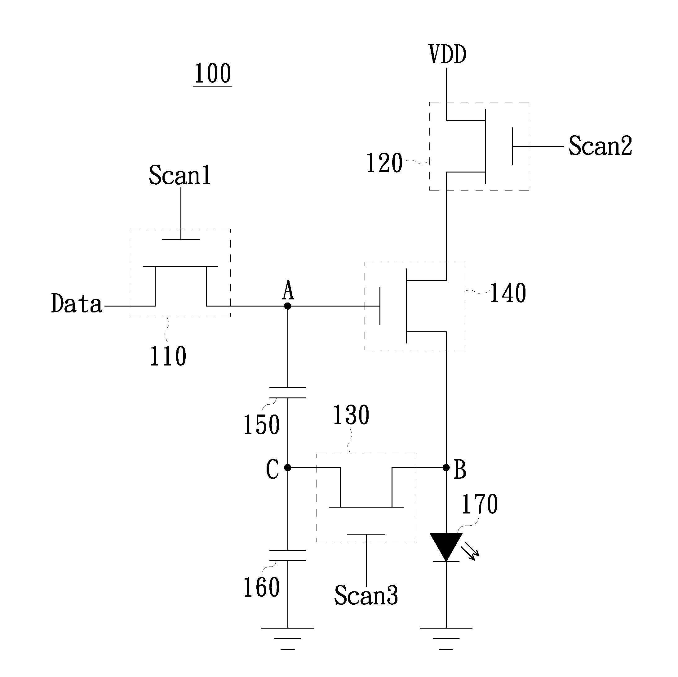
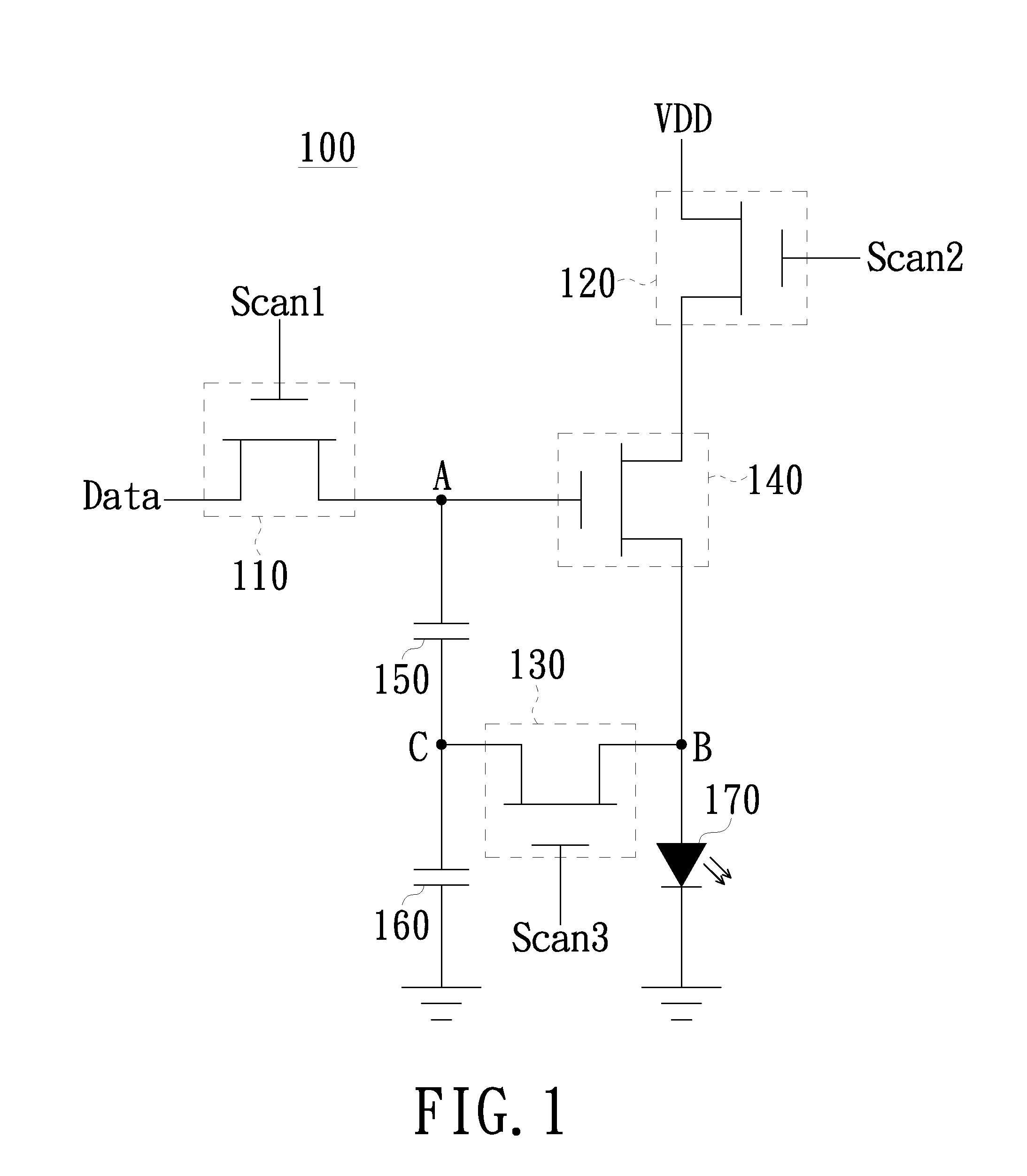
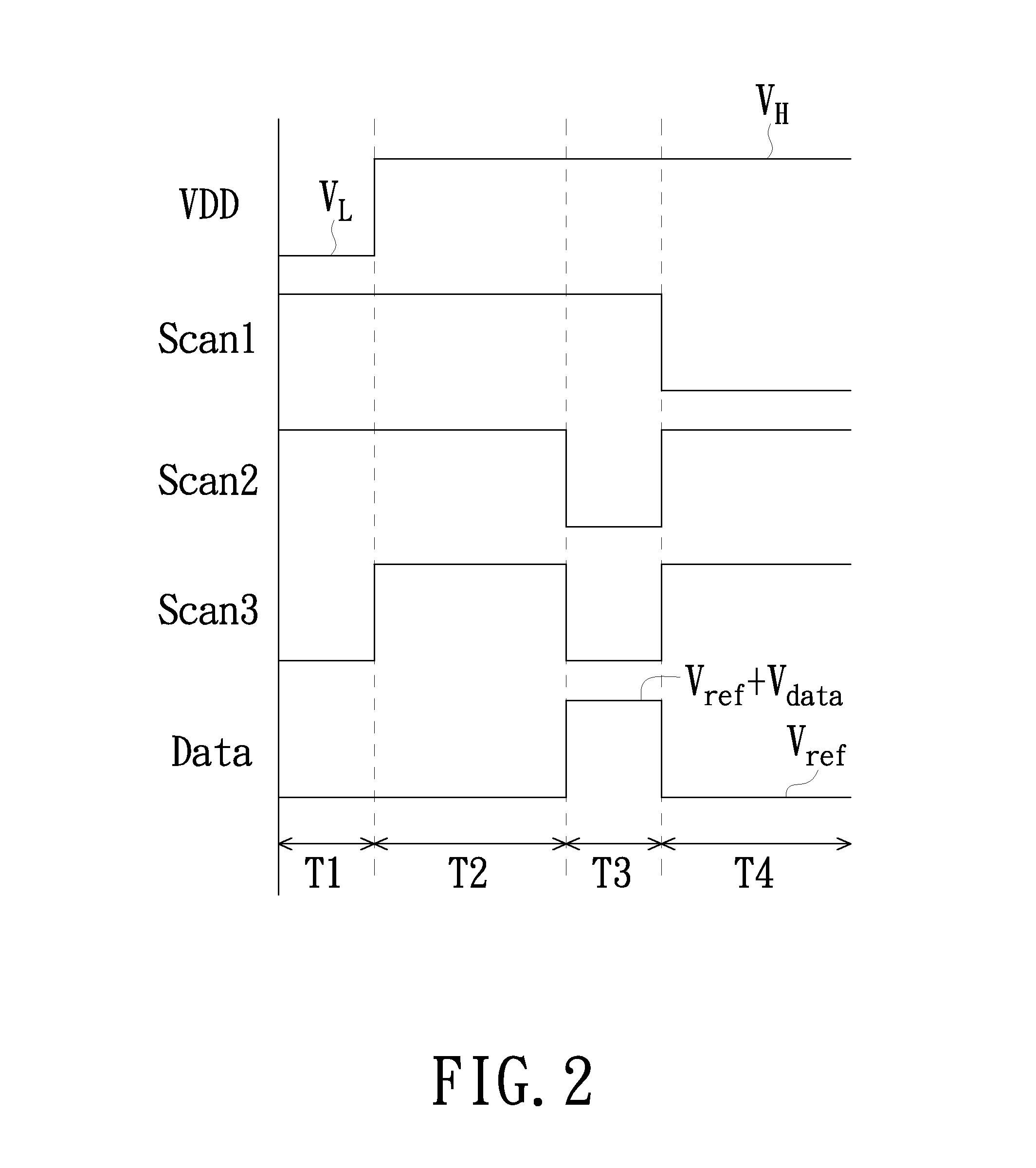
[0014]Please refer to FIG. 1, which is a schematic pixel circuit diagram in accordance with the present invention, As shown in FIG. 1 the pixel circuit 100 in the present embodiment includes a first switch 110, a second switch 120, a third switch an N-type transistor 140 (functioned as a driving transistor in one embodiment), a first capacitor 150, a second capacitor 160 and an organic light emitting diode (OLED) 170, The first switch 110 has a first control end, a first end and a second end. The first switch 110 is configured to have the first control end electrically coupled to a first scan line (not shown) and the first end for receiving a data signal Data. The second switch 120 has a second control end, a third end and a fourth end. The second switch 120 is configured to have the second control end electrically coupled to a second scan line not shown) and the third end for receiving a power supply voltage VDD. The N-type transistor 140 has a third control end, a fifth end and a ...
second embodiment
[0021]Please refer to FIG. 3, which is a schematic pixel circuit diagram in accordance with the present invention. Elements or signals in the pixel circuit 200 in FIG. 3 of the present: embodiment that are identical to those shown in FIG. 1 are labeled with the same numberings for simplification. The main difference between the pixel circuit 200 in FIG. 3 and the pixel circuit 100 in FIG. 1 is that the control end of the third switch 130 is configured to receive the second scan signal Scan2 through the third scan line (not shown). Thus, the third switch 130 is configured to be turned either ON or OFF according to the second scan signal Scan2. Similarly, in the present embodiment, the first reference voltage level is implemented by a ground voltage level; however, the present invention is not limited thereto. Further, in the present embodiment, the first switch 110, second switch 120 and third switch 130 are each implemented by an N-type transistor, and the pixel circuit 200 in the p...
PUM
 Abstract
Description
Claims
Application Information
 - R&D
- Intellectual Property
- Life Sciences
- Materials
- Tech Scout
- Unparalleled Data Quality
- Higher Quality Content
- 60% Fewer Hallucinations
Browse by: Latest US Patents, China's latest patents, Technical Efficacy Thesaurus, Application Domain, Technology Topic, Popular Technical Reports.
© 2025 PatSnap. All rights reserved.Legal|Privacy policy|Modern Slavery Act Transparency Statement|Sitemap|About US| Contact US: help@patsnap.com


