Measuring individual device degradation in CMOS circuits

a technology of cmos circuits and individual devices, applied in measurement devices, semiconductor operation lifetime testing, instruments, etc., can solve the problems of reducing the drain current of the device, and still degrading the circuit by a significant and measurable amoun

Active Publication Date: 2017-03-02
IBM CORP
View PDF2 Cites 5 Cited by
  • Summary
  • Abstract
  • Description
  • Claims
  • Application Information

AI Technical Summary

Benefits of technology

[0007]A test oscillator includes multiple oscillator stages, with each stage having a delay stage and one or more fan-out devices to simulate a load, and a test stage that includes a delay stage and a test device having an input terminal for measuring one or more electrical properties of the test device. The plurality of oscillator stages and the test stage are arranged linearly, with a final stage feeding back into a first stage to provide oscillation.
[0008]A method of measuring degradation includes measuring an initial electrical characteristic of a test device in a ring oscillator that includes multiple oscillator stages, each having a delay stage and one or more fan-out devices, and a test stage having a delay stage and the test device. The ring oscillator is operated for a period of time. The electrical characteristic of the test device is measured after operating the ring oscillator. A level of degradation in the test device is determined using a processor based on the measurements of the electrical characteristic of the test device.

Problems solved by technology

While efforts have been made to minimize the degradation, circuits are still degraded by a significant and measurable amount in operation, and therefore prediction of the amount of degradation which will occur during the expected lifetime of a device is still needed.
Bias-temperature instability (BTI) produces increases in the threshold voltage of a semiconductor device and therefore reduces the drain current of the device.
The progression of BTI degradation is determined by total power-on time of the device and is a result of charge carriers tunneling through barriers and damaging the material along interfaces.
For example, in some devices, such as p-type FETs, BTI degrades the conducting channel-to-dielectric interface, creating interface traps that reduce transisitor performance.
In both cases, BTI and HCI cause physical damage to the device and will eventually change the properties of the device.
Both types of degradation occur naturally during operation of the devices at normal conditions, and can be made to occur more rapidly by raising the temperature and voltages applied to the devices.
The degradation of individual FETs results in reduced propagation speed in logic circuits.
However, the net frequency reduction does not reveal which particular transistors (e.g., n-type or p-type FETs) in a circuit have aged the most, nor does it reveal what the changes in their characteristics are, nor whether the mechanism is predominately reverse bias-temperature instability (BTI) or hot carrier injection (HCI) damage.

Method used


Image

  • Measuring individual device degradation in CMOS circuits
  • Measuring individual device degradation in CMOS circuits
  • Measuring individual device degradation in CMOS circuits

Examples


Embodiment Construction

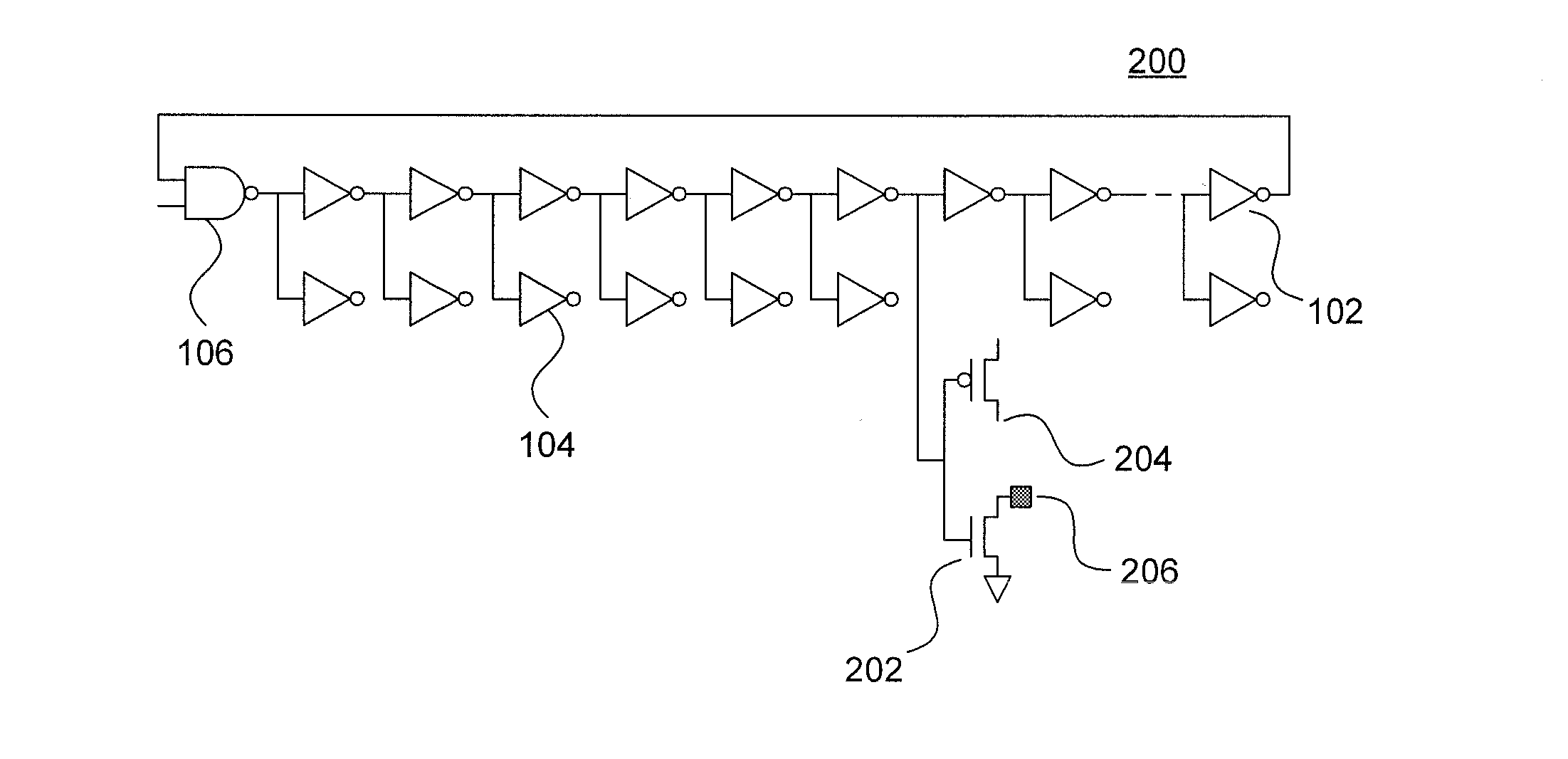
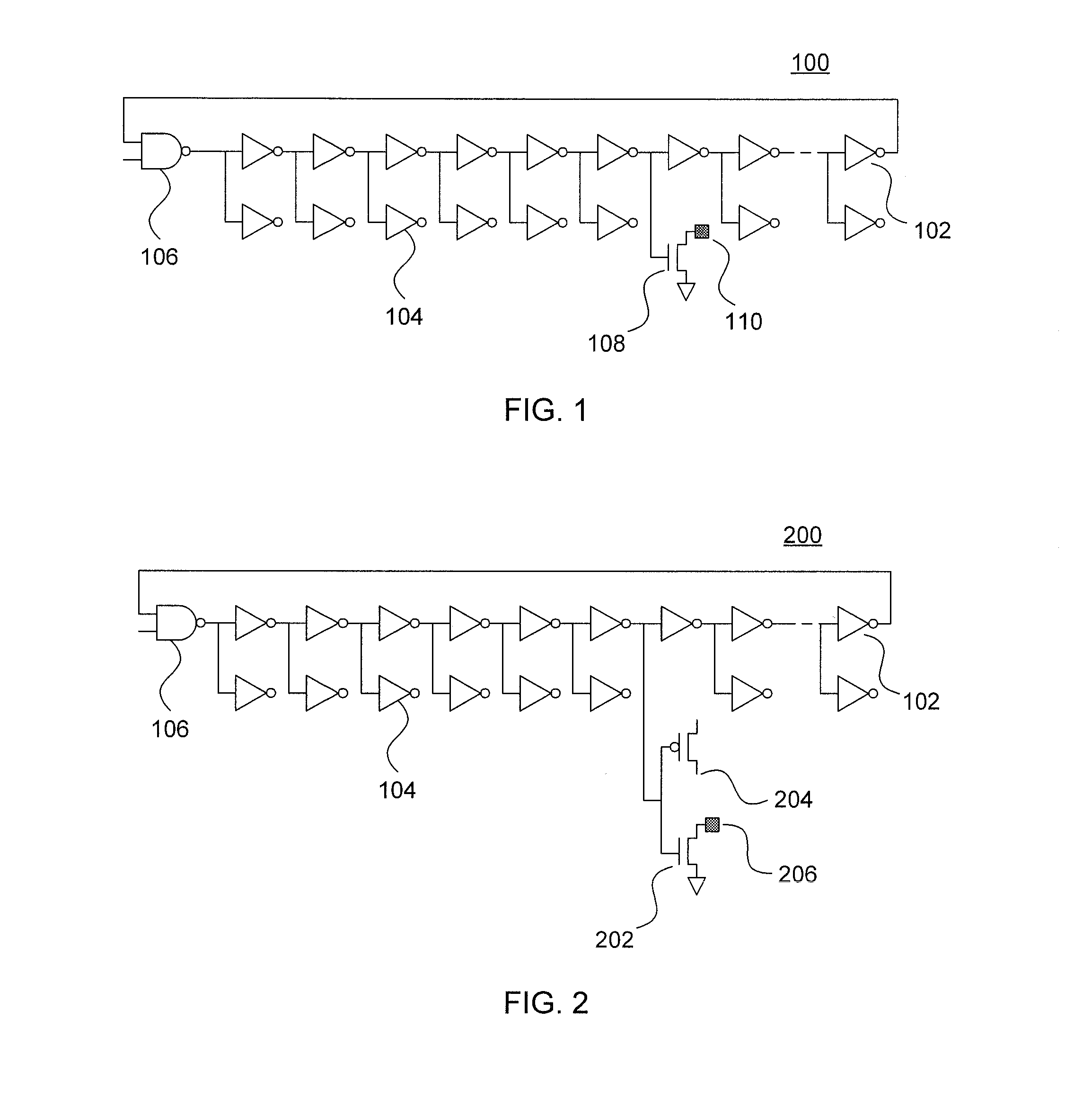
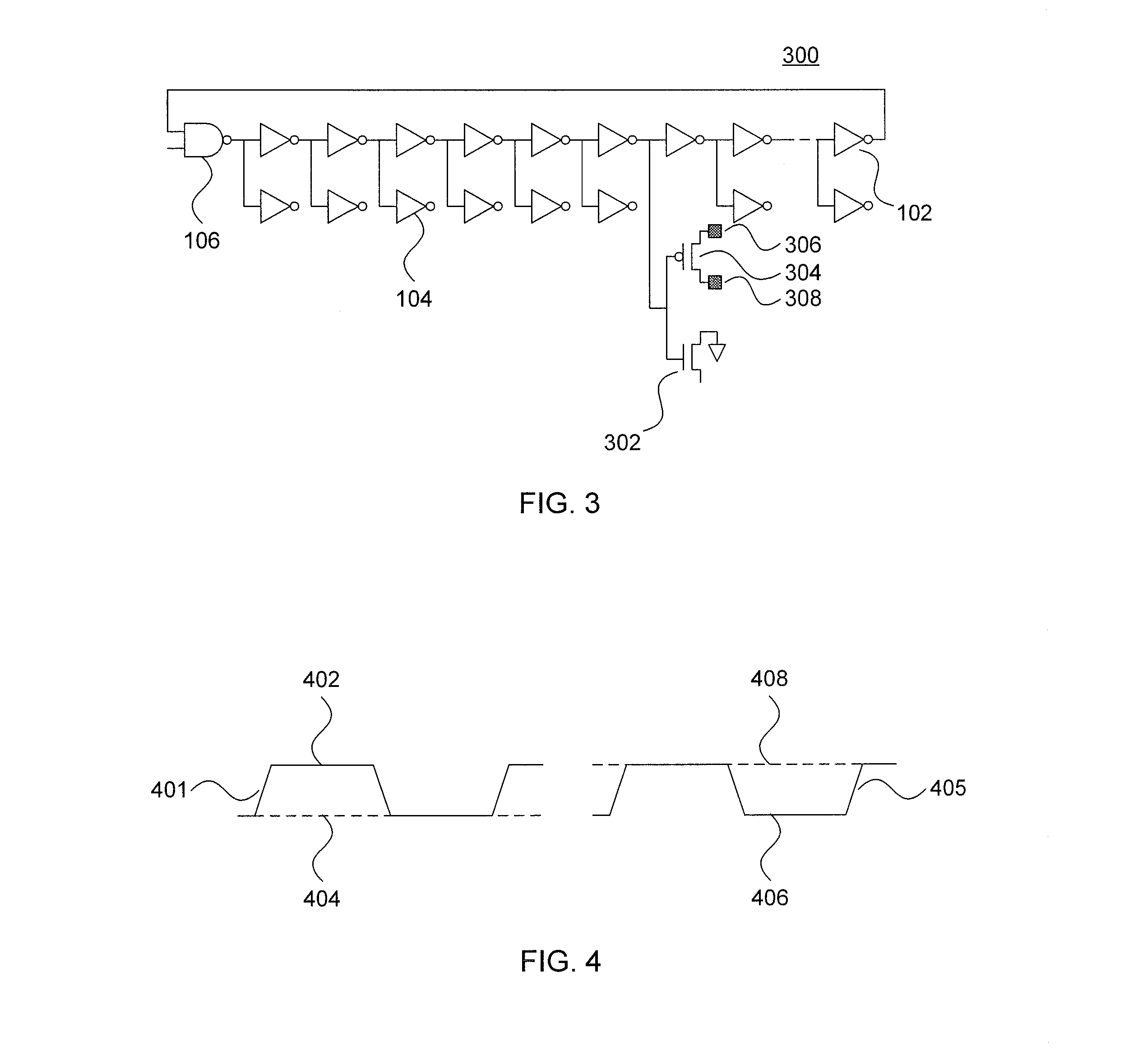
[0024]Embodiments of the present principles measure individual device characteristics in a degraded ring oscillator or delay chain. By replacing a fan out device on one stage of the ring oscillator or delay chain with a test device and access point, the test device experiences the same gate signal as the circuit elements, but its individual characteristics (such as drain current and threshold voltage) can be measured. The test device can be n-type field effect transistors (FETs) or p-type FETs, and can be subjected to bias temperature instability (BTI) stress only, or to a combination of BTI and hot carrier injection (HCI) stress. The biases applied to the source and drain terminals of the FETs determine if the gate voltage induces BTI stress or HCI stress or both. BTI stress occurs when the FET gate is biased with respect to its source and drain, while HCI stress can only occur if the source and drain are at different potentials, allowing channel current to flow.

[0025]Referring now...


PUM


Abstract

Methods and systems for measuring degradation includes measuring an initial electrical characteristic of a test device in a ring oscillator that includes multiple oscillator stages, each having a delay stage and one or more fan-out devices, and a test stage having a delay stage and the test device. The ring oscillator is operated for a period of time. The electrical characteristic of the test device is measured after operating the ring oscillator. A level of degradation in the test device is determined using a processor based on the measurements of the electrical characteristic of the test device.

Description

BACKGROUND[0001]Technical Field[0002]The present invention relates to measuring device degradation and, more particularly, to measuring degradation characteristics of individual devices when a circuit degrades from normal or stressed operation.[0003]Description of the Related Art[0004]Degradation of the electrical properties of field complementary metal-oxide semiconductor (CMOS) field effect transistors (FETs) is a consequence of their operation. While efforts have been made to minimize the degradation, circuits are still degraded by a significant and measurable amount in operation, and therefore prediction of the amount of degradation which will occur during the expected lifetime of a device is still needed.[0005]Bias-temperature instability (BTI) produces increases in the threshold voltage of a semiconductor device and therefore reduces the drain current of the device. The progression of BTI degradation is determined by total power-on time of the device and is a result of charge ...

Claims


Application Information

Patent Timeline
Patent Type & Authority Applications(United States)
IPC IPC(8): G01R31/26
CPCG01R31/2621G01R31/2642G01R31/2884
Inventor LINDER, BARRY P.JENKINS, KEITH A.
Owner IBM CORP
Why Eureka
Try Eureka