Semiconductor structure

a technology of semiconductors and structures, applied in the direction of semiconductor devices, basic electric elements, electrical equipment, etc., can solve the problems of high contact resistance, failure of devices, and inability to achieve insulating cap layers, so as to prevent shorting and lower contact resistance

Active Publication Date: 2017-03-16
UNITED MICROELECTRONICS CORP
View PDF63 Cites 8 Cited by
  • Summary
  • Abstract
  • Description
  • Claims
  • Application Information

AI Technical Summary

Benefits of technology

[0008]One objective of the present invention is to provide a semiconductor structure which is able to prevent shorting between the S / D contact plug and the gate. The proposed semiconductor structure also provides a larger landing area for the gate contact plug with lower contact resistivity as a consequence.

Problems solved by technology

Conventional contact forming processes have frequently been found to cause issues such as electric shorting between the gate and an S / D contact of a transistor, as well as high contact resistivity resulting from the smaller CD and smaller landing area of the gate contact plug.
Those problems may cause failure of the device.
The insulating cap layer is not desirable for the gate contact plug, however, as it may cause extra difficulty for the gate contact hole etching.

Method used


Image

  • Semiconductor structure
  • Semiconductor structure
  • Semiconductor structure

Examples


Embodiment Construction

[0020]In the following description, numerous specific details are given to provide a thorough understanding of the invention. It will, however, be apparent to one skilled in the art that the invention may be practiced without these specific details. Furthermore, some system configurations and process steps are not disclosed in detail, as these should be well-known to those skilled in the art. Other embodiments may be utilized, and structural, logical, and electrical changes may be made without departing from the scope of the present invention.

[0021]The drawings showing embodiments of the apparatus are semi-diagrammatic and not to scale, and some dimensions are exaggerated in the figures for clarity of presentation. Where multiple embodiments are disclosed and described as having some features in common, like or similar features will usually be described with like reference numerals for ease of illustration and description thereof.

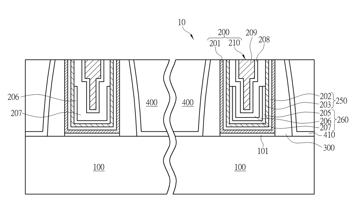
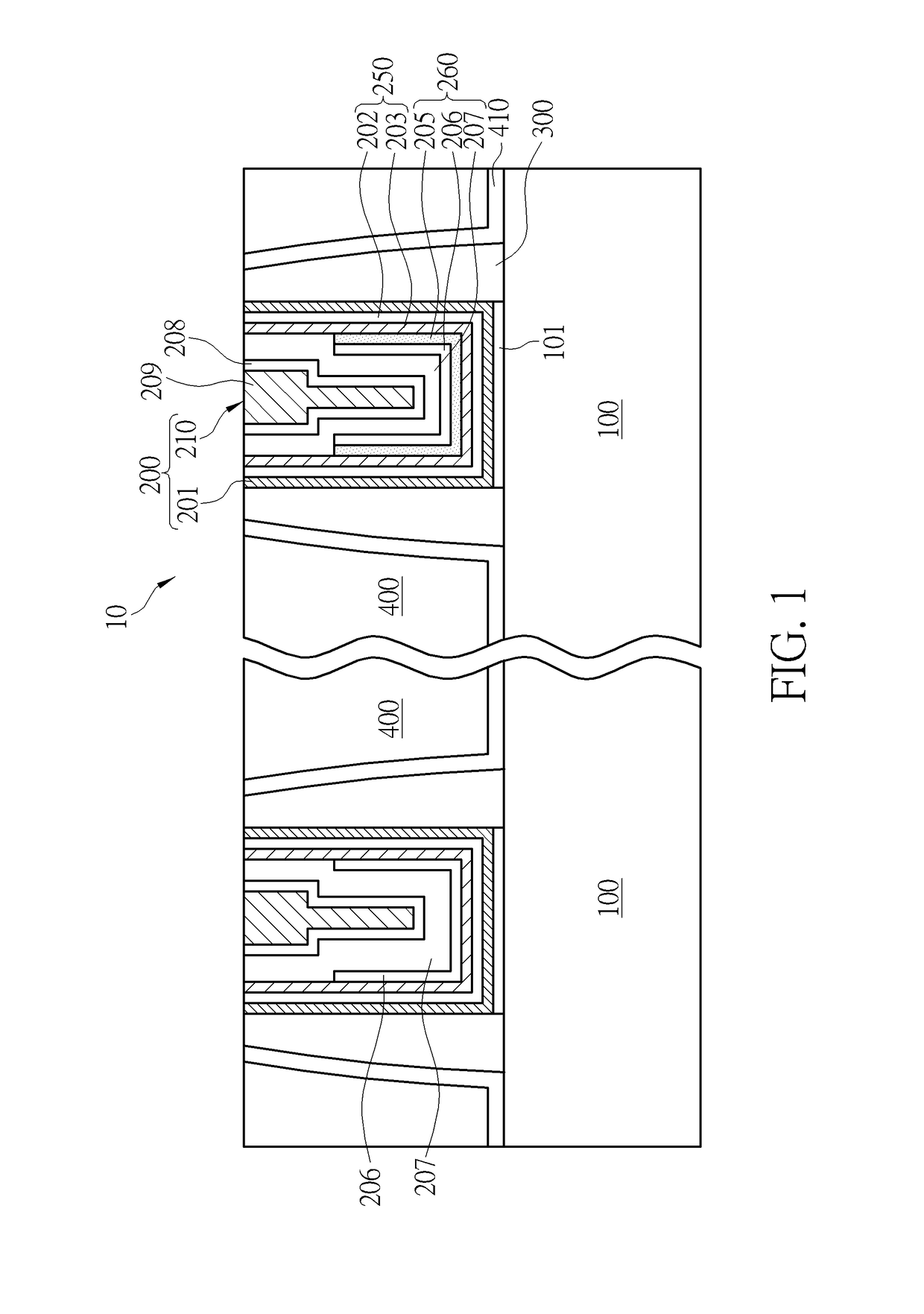
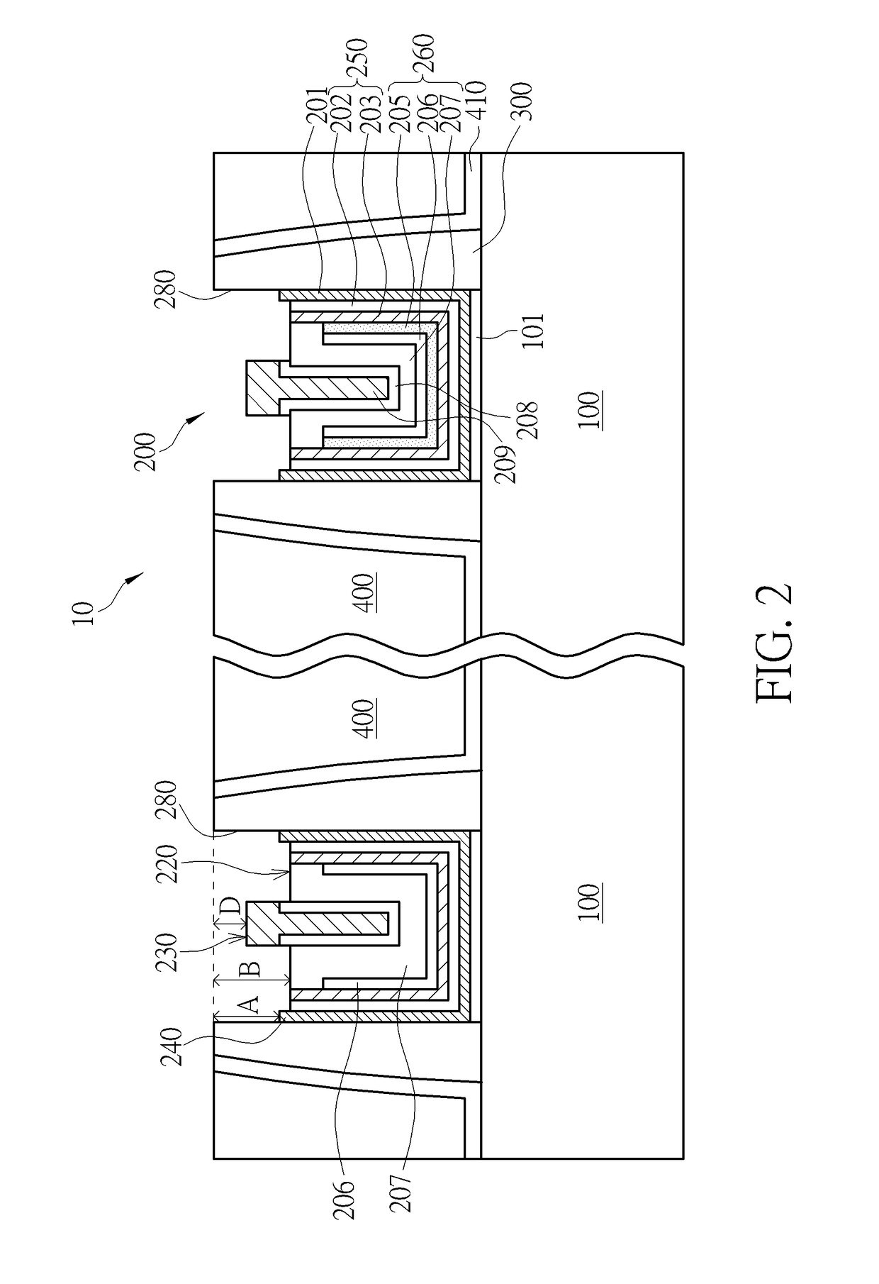
[0022]FIGS. 1-4 are schematic cross-sectional diagram...


PUM

PropertyMeasurementUnit
semiconductoraaaaaaaaaa
semiconductor structureaaaaaaaaaa
work functionaaaaaaaaaa

Abstract

A semiconductor structure is disclosed. The semiconductor structure includes a substrate, and an interlayer dielectric disposed on the substrate which has agate structure therein. The gate structure further includes a gate electrode with a protruding portion, and a gate dielectric layer disposed between the gate electrode and the substrate. A spacer is disposed between the interlayer dielectric and the gate electrode. An insulating cap layer is disposed atop the gate electrode and encompasses the top and the sidewall of the protruding portion.

Description

BACKGROUND OF THE INVENTION[0001]1. Field of the Invention[0002]The invention generally relates to a semiconductor structure. More particularly, the invention relates to a structure with an insulating cap layer.[0003]2. Description of the Prior Art[0004]In the field of semiconductor manufacturing, after a transistor structure is formed, conductive contact plugs are formed to make the transistor fully functional. Source / drain contact (S / D contact) plugs connect to the source and drain region of the transistor, and gate contact plugs connect to the gate of the transistor.[0005]With the continuous scaling down of chip size, the critical dimension (CD) and spacing of these contact plugs is becoming smaller. Conventional contact forming processes have frequently been found to cause issues such as electric shorting between the gate and an S / D contact of a transistor, as well as high contact resistivity resulting from the smaller CD and smaller landing area of the gate contact plug. Those ...

Claims


Application Information

Patent Timeline
Patent Type & Authority Applications(United States)
IPC IPC(8): H01L29/49H01L29/423
CPCH01L29/42376H01L29/4966H01L29/0649H01L29/42364
Inventor HUNG, CHING-WENHUANG, CHIH-SENCHEN, YI-WEILIN, CHUN-HSIEN
Owner UNITED MICROELECTRONICS CORP
Why Eureka
Try Eureka