High frequency light emission device

a light emission device and high frequency technology, applied in the field of light emission devices, can solve the problems of too slow rate at which light can be modulated (alternating, states) and cannot be used in any communication or data processing application, and achieve the effect of easy local integration

Inactive Publication Date: 2017-03-23
BROWN UNIVERSITY
View PDF29 Cites 6 Cited by
  • Summary
  • Abstract
  • Description
  • Claims
  • Application Information

AI Technical Summary

Benefits of technology

[0005]This invention addresses the issue of direct modulation of long lifetime light emitters. The present invention enables one to realize new nanometer-scale architecture for on-chip ultrafast directly modulated light sources, which could be easily integrated locally on a range of nanoelectronic and nanophotonic structures. Additional structures, such as light-emitting diodes, waveguides, and fibers for use in fiber optic communication are also available. For example, direct, electrical, sub-lifetime modulation of light emission has direct applications at the interface of communication, display, and lighting technologies as well as in biological and chemical sensing.

Problems solved by technology

Indeed, when one pumps the electronic system governing light emission from such a quantum emitter, the rate at which light can be modulated (alternating from ‘ON’ and ‘OFF’ states) is limited by the lifetime of emission.
Such a rate is too slow to be used for any communication or data processing applications.
Such a two-step two devices scheme requires a large footprint (generally hundreds of μm2) which makes it challenging for future scalability at the nanoscale; it also constitutes a low efficiency system as much of the light must be “thrown out” in the modulation process.

Method used


Image

  • High frequency light emission device
  • High frequency light emission device
  • High frequency light emission device

Examples


Embodiment Construction

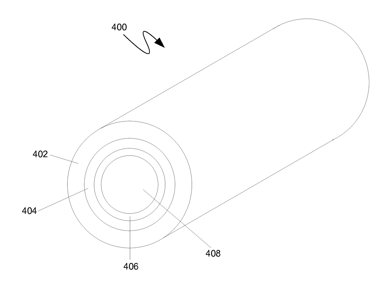
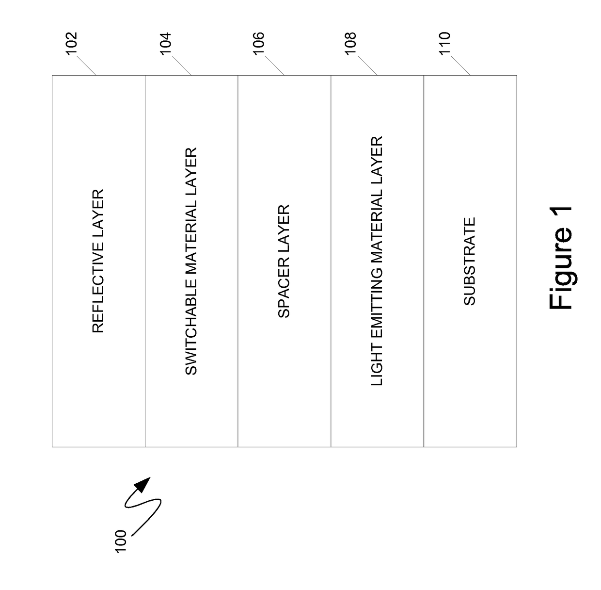
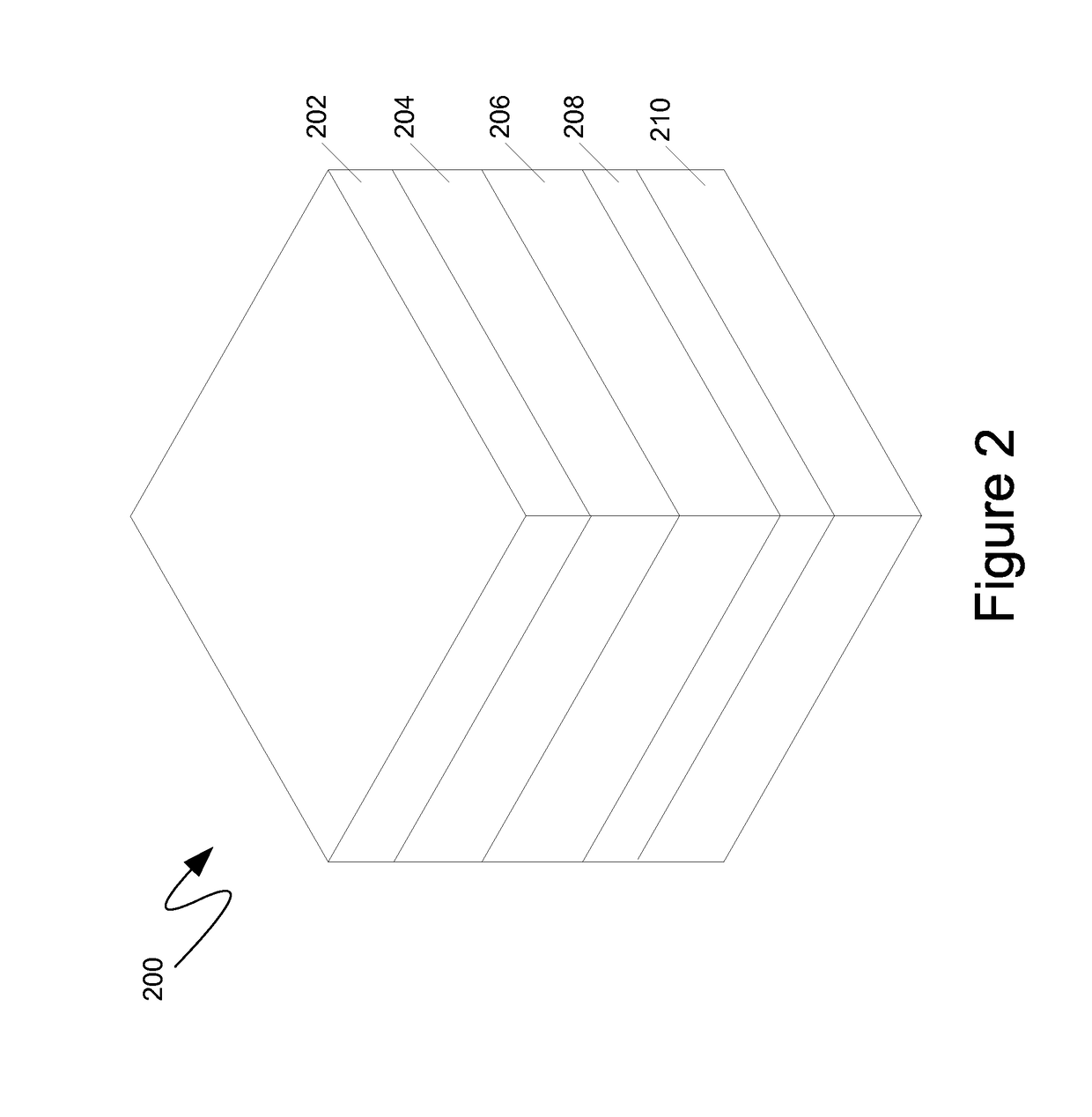
[0013]As mentioned above, the long lifetimes of certain light emitters, such as lanthanide and transition-metal phosphors or emitters, present challenges for conventional pump-based modulation methods where the maximum switching speeds are limited by the decay time of the excited state. While these light emitters have longer lifetimes, they are also efficient light emitters and often play a role in a range of modern device technologies from displays and lighting to lasers, sensors, and telecommunication. Nevertheless, their slow radiative decay rate is generally perceived as a technological limit for high-speed photonic devices. This is particularly problematic for transition-metal and lanthanide phosphors, such as erbium-doped materials, as they have lifetimes on the order of milliseconds to hundreds of microseconds, which would appear to restrict modulation speeds to the range of 1-10 kHz. To overcome this limit, the present application discloses methods and systems for directly m...


PUM

PropertyMeasurementUnit
thickaaaaaaaaaa
thickaaaaaaaaaa
thickaaaaaaaaaa

Abstract

Systems, apparatuses, and methods for modulating light at high frequencies by addressing the issue of direct modulation of long lifetime light emitters. Dynamic control of the local density of optical states (LDOS) to exploit the differences between electric and magnetic dipole transitions allows for higher frequency modulation. The LDOS is controlled, in part, by designing a structure such that it enhances or suppresses electric and magnetic dipoles. Direct modulation may be achieved by designing the optical environment to adjust the interferences between the emitted light field and its own reflection at the emitter's location. The optical environment may include light emission material, switchable material, spacer materials, and reflective materials. The structures creating the optical environment enable a new nanometer-scale architecture for on-chip ultrafast directly modulated light sources, which could be easily integrated locally on a range of nanoelectronic and nanophotonic structures, along with light-emitting diodes, waveguides, and fiber optics.

Description

CROSS REFERENCE TO RELATED APPLICATIONS[0001]The application claims priority to U.S. Provisional Application Ser. No. 61 / 970,234, titled “HIGH FREQUENCY LIGHT EMISSION DEVICE,” which is incorporated herein by reference in its entirety.STATEMENT REGARDING FEDERALLY SPONSORED RESEARCH OR DEVELOPMENT[0002]This invention was made with government support under ECCS-0846466 and awarded by the National Science Foundation and FA9550-10-1-0026 awarded by the Air Force Office of Sponsored Research. The government has certain rights in the invention.TECHNICAL FIELD[0003]The present disclosure provides a light emission device that can be directly modulated at a very high rate of speed. The device has a number of applications including, but not limited to, applications in optical data transmission. Related methods are also provided.INTRODUCTION[0004]Direct modulation of light emission is usually believed to be limited by the intrinsic spontaneous emission rate of a light emitter. Indeed, when on...

Claims


Application Information

Patent Timeline
Patent Type & Authority Applications(United States)
IPC IPC(8): G02F1/01G02F1/00H04B10/50H01L33/58H01L33/60
CPCG02F1/0115H01L33/58H01L33/60G02F2203/50G02F1/011G02F1/0018G02F2201/34H04B10/502H01L33/0004H01L33/24
Inventor ZIA, RASHIDCUEFF, SEBASTIENKARAVELI, SINAN
Owner BROWN UNIVERSITY
Why Eureka
Try Eureka