Composite wafer semiconductor devices using offset via arrangements and methods of fabricating the same

Active Publication Date: 2017-03-30
SAMSUNG ELECTRONICS CO LTD
View PDF3 Cites 57 Cited by
  • Summary
  • Abstract
  • Description
  • Claims
  • Application Information

AI Technical Summary

Benefits of technology

[0006]Some embodiments of the inventive concept provide semiconductor devices having an I/O in

Problems solved by technology

To satisfy these technical requirements, complexity and/or int

Method used


Image

  • Composite wafer semiconductor devices using offset via arrangements and methods of fabricating the same
  • Composite wafer semiconductor devices using offset via arrangements and methods of fabricating the same
  • Composite wafer semiconductor devices using offset via arrangements and methods of fabricating the same

Examples


Embodiment Construction

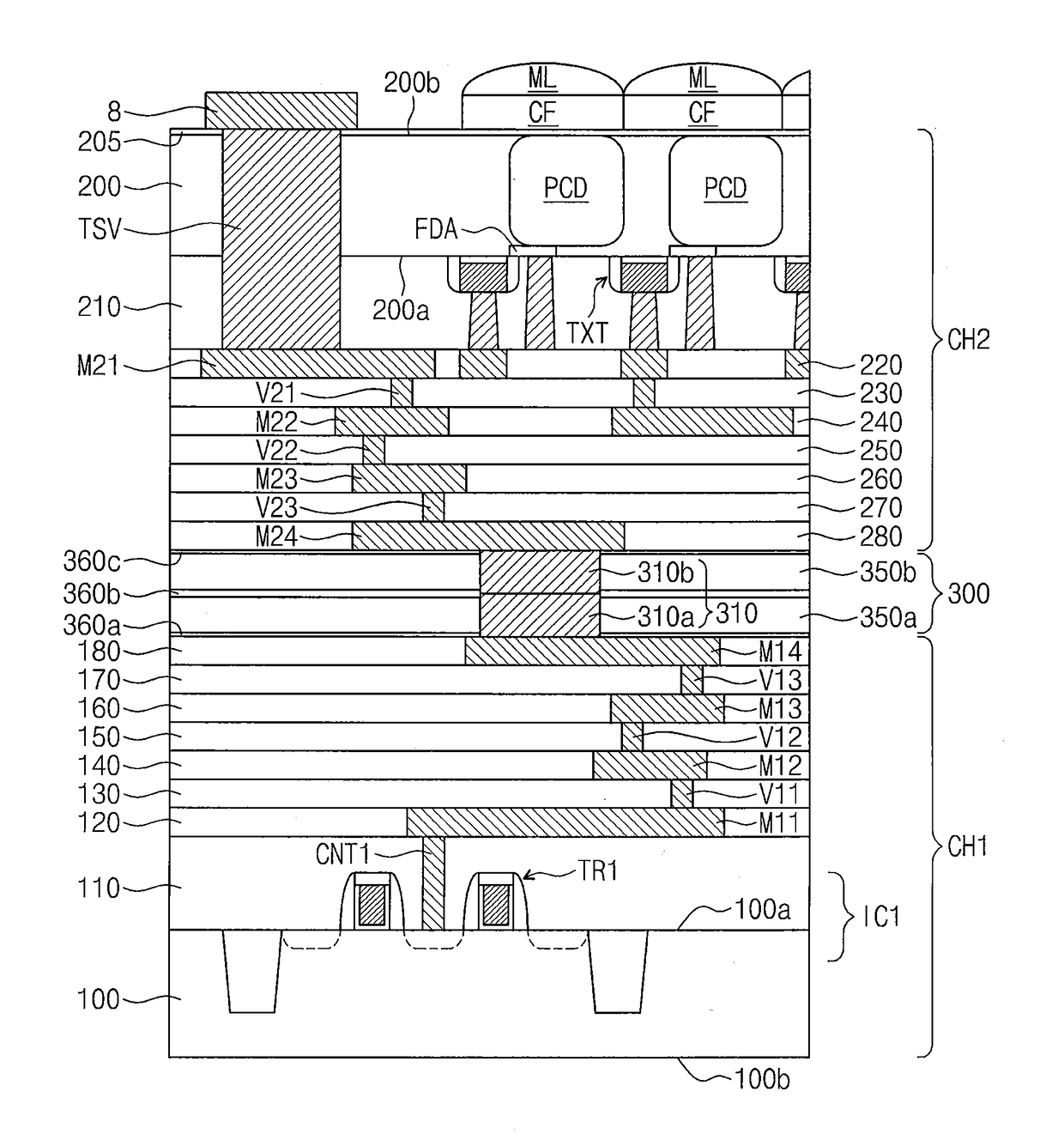
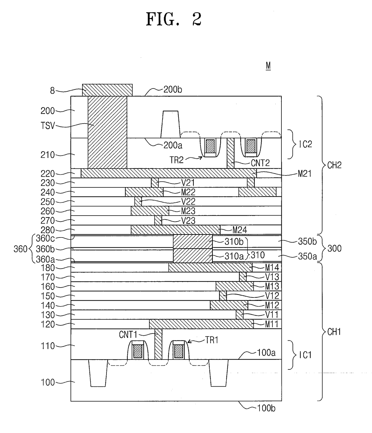
[0037]The inventive concepts will now be described more fully hereinafter with reference to the accompanying drawings, in which exemplary embodiments of the inventive concepts are shown. The inventive concepts and methods of achieving them will be apparent from the following exemplary embodiments that will be described in more detail with reference to the accompanying drawings. The embodiments of the inventive concept may, however, be embodied in different forms and should not be constructed as limited to the embodiments set forth herein. Rather, these embodiments are provided so that this disclosure will be thorough and complete, and will fully convey the scope of the inventive concept to those skilled in the art.

[0038]As used herein, the singular terms “a,”“an” and “the” are intended to include the plural forms as well, unless the context clearly indicates otherwise. It will be understood that when an element is referred to as being “connected” or “coupled” to another element, it ...


PUM


Abstract

A device includes a first integrated circuit substrate including a plurality of first metal layers interconnected by first vias and a second integrated circuit substrate on the first integrated circuit substrate and including second metal layers interconnected by second vias. An insulation layer is disposed between the first and second substrates and a connection region is disposed in the insulation layer and electrically connects a first one of the first metal layers to a first one of the second metal layers. The device further includes a bonding pad on the second substrate and a through via extending from the bonding pad and into the second to contact a second one of the second metal layers. The through via is positioned so as to not overlap at least one of the first vias, the second vias and the connection region. Methods of fabricating such device are also described.

Description

CROSS-REFERENCE TO RELATED APPLICATIONS[0001]This U.S. non-provisional patent application claims priority under 35 U.S.C. §119 to Korean Patent Application No. 10-2015-0135840, filed on Sep. 24, 2015, in the Korean Intellectual Property Office, the entire contents of which are hereby incorporated by reference.BACKGROUND OF THE INVENTION[0002]The present disclosure relates to semiconductor devices and methods of fabricating the same and, more particularly, to semiconductor devices including semiconductor chips stacked at a wafer level stage and methods of fabricating the same.[0003]Due to their small-size, multifunctionality, and / or low-cost characteristics, semiconductor devices are considered important elements in the electronic industry. The semiconductor devices may be classified into a memory device for storing data, a logic device for processing data, and a hybrid device including both of memory and logic elements. Due to the increased demand for electronic devices with fast sp...

Claims


Application Information

Patent Timeline
IPC IPC(8): H01L27/146H04N5/378H04N5/225
CPCH01L27/14634H01L27/1469H01L27/1464H01L27/14645H01L27/14621H04N5/378H01L27/1462H01L27/14636H01L27/14618H04N5/2253H04N5/2254H01L27/14627H01L23/5384H01L25/043H01L27/14601H01L27/14683H01L2224/48091H01L2224/48237H01L2224/73265H01L2924/15311H01L28/00H01L23/481H01L23/5226H01L25/0657H01L2225/0651H01L2225/06513H01L25/18H04N23/54H10B43/27H01L2924/00014H01L2224/32146H01L2225/06544H01L24/32H01L2224/32105H01L23/49827H01L25/065
Inventor KWON, DOOWON
Owner SAMSUNG ELECTRONICS CO LTD
Why Eureka
Try Eureka