Eureka AIR delivers breakthrough ideas for toughest innovation challenges, trusted by R&D personnel around the world.

Array substrate apparatus applying the same and assembly method thereof

a technology of array substrate and substrate, applied in the field of substrate and display apparatus, can solve the problems of not being able to minimize the dimension of the array substrate, the evaporation process used to form the amoled display still has some technical problems to be solved, and the portability device applying the tft-lcd may not be so eco-friendly, etc., to achieve the effect of simple assembly process, high luminous efficiency and thin thickness

Active Publication Date: 2017-04-13
INNOLUX CORP
View PDF1 Cites 27 Cited by
  • Summary
  • Abstract
  • Description
  • Claims
  • Application Information

AI Technical Summary

Benefits of technology

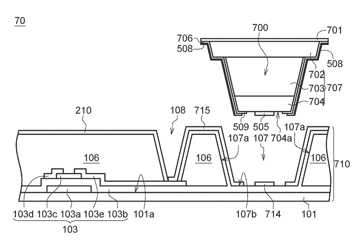
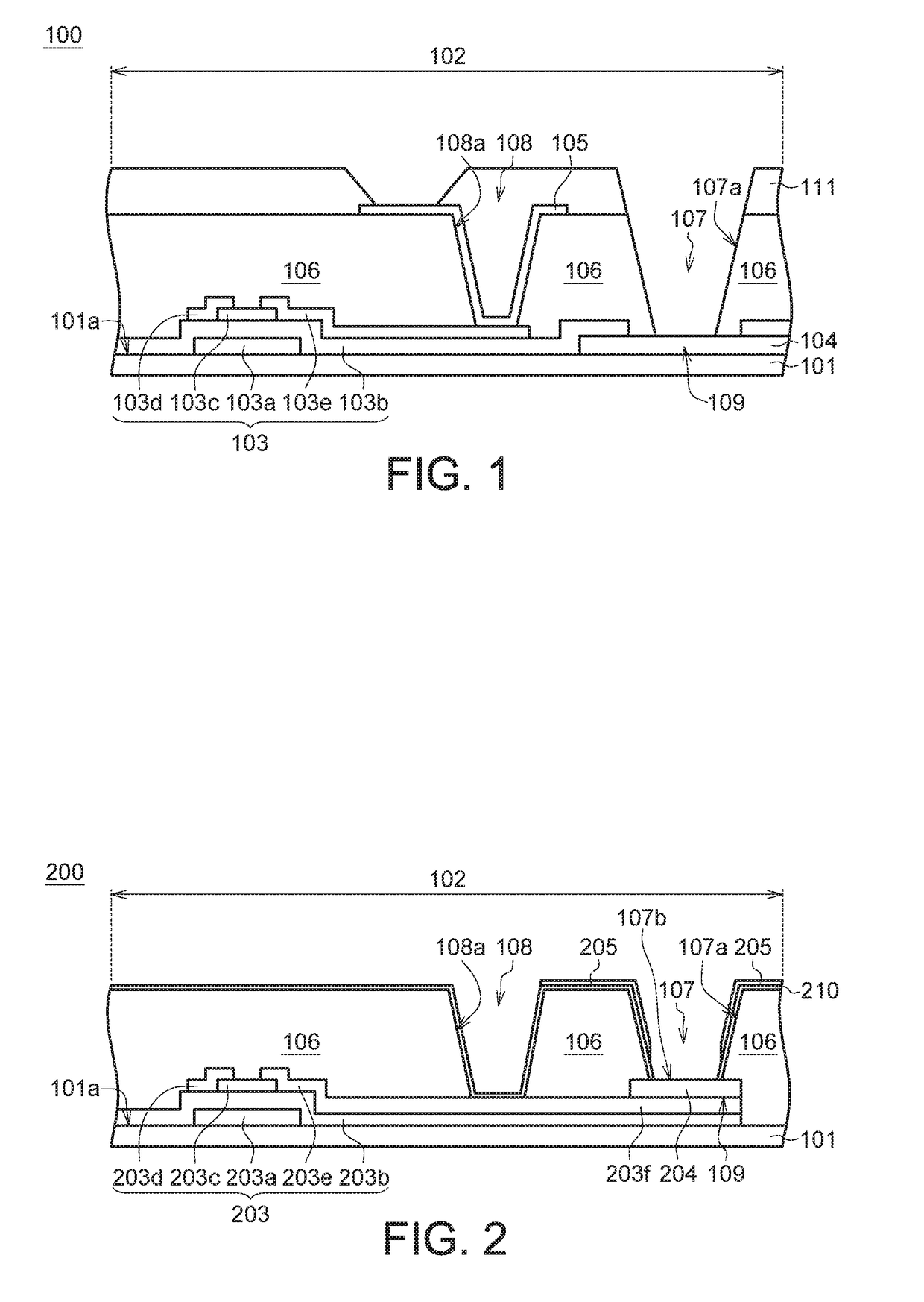
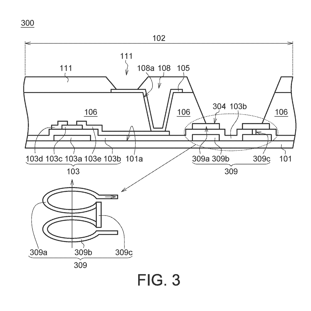
The present patent provides an eco-friendly display apparatus with high luminous efficiency and thin thickness, by using surface mounting technology to assemble a plurality of LEDs onto an array substrate without applying liquid crystal molecule. The LEDs and array substrate are self-aligned by magnetic force formed there between, thus the process for assembling the same does not require an align mark. This simplifies the process for assembling the LEDs and array substrate and reduces manufacturing cost of the display apparatus. A pre-alignment step can be performed to improve the alignment accuracy between the LEDs and the array substrate by using a metal plate.

Problems solved by technology

The portable devices applying the TFT-LCD may not be so eco-friendly due to the use of the liquid crystal, and the dimension thereof may not be minimized due to the additional thickness of the backlight module.
However, the evaporation process used to form the AMOLED displays still has some technical problems to be solved.
Besides, the long-standing problems, including materials aging and non-uniform illumination, may also adversely affect the performance of the AMOLED displays.
Such that, the process for fabricating the AMOLED displays may have poor yield and product reliability.
Such that, the long-standing problems of the AMOLED displays, including materials aging, non-uniform illumination, poor yield and product reliability, can be obviated.

Method used


Image

  • Array substrate apparatus applying the same and assembly method thereof
  • Array substrate apparatus applying the same and assembly method thereof
  • Array substrate apparatus applying the same and assembly method thereof

Examples


Embodiment Construction

[0025]The disclosure provides an array substrate, a display apparatus applying the same and the assembly method thereof to form a more eco-friendly display apparatus with high luminous efficiency and thin thickness and to obviate the long-standing problems of non-uniform illumination, poor yield and product reliability resulted from a conventional AMOLED display. To make the objects, technical features and advantages of the disclosure more apparent and easily understood, a number of exemplary embodiments are exemplified below with accompanying drawings.

[0026]It should be noted that the implementations and methods disclosed in the present disclosure are not for limiting the invention. The invention still can be implemented by using other features, elements methods and parameters. Exemplary embodiments are provided for illustrating the technical features of the invention, not for limiting the scope of protection of the invention. Any persons ordinarily skilled in the art can make suit...


PUM


Abstract

An array substrate, a display apparatus applying the same and the assembly method thereof are provided, wherein the array substrate includes a substrate having a plurality of pixels, each of the pixels at least includes a thin film transistor (TFT) device, a first electrode, a second electrode separated from the first electrode all of which are disposed on the substrate. at least one of the first electrode and the second electrode is electrically contacted to the TFT device, and either the first electrode or the second electrode has a magnetic force generator used to generate a magnetic force substantially ranging from 10 gauss to 1000 gauss.

Description

[0001]This application claims the benefit of People's Republic of China application Serial No. 201510648262.3, filed Oct. 9, 2015, the subject matter of which is incorporated herein by reference.BACKGROUND[0002]Field of the Invention[0003]The disclosure relates in general to a substrate, a display apparatus applying the same and the assembly method thereof, and more particularly to an array substrate, a display apparatus applying the same and the assembly method thereof.[0004]Description of the Related Art[0005]With the development of electronic technology, the design trend of next-generation portable devices may focus on features of eco-friendly solutions, light weight, thin thickness, lower power consumption, higher resolution and higher performance. A thin film transistor liquid crystal display (TFT-LCD) having advantages of high luminous efficiency, long service life and durable has been broadly applied to the portable devices. However, because the response of liquid crystal mol...

Claims


Application Information

Patent Timeline
Patent Type & Authority Applications(United States)
IPC IPC(8): H01L27/12H01L27/32H01L29/45
CPCH01L27/124H01L27/3276H01L27/1259H01L29/458H01L21/50H01L27/1255H01L27/156H10K59/131H10K59/805H10K50/805
Inventor PENG, JEN-CHIENTSAI, CHIA-HAOHSIEH, TSAU-HUA
Owner INNOLUX CORP
Why Eureka
Eureka Blog
Learn More