System in package

a technology of electrical package and package, applied in the direction of semiconductor devices, semiconductor/solid-state device details, electrical apparatus, etc., can solve problems such as bulky electronic systems

Active Publication Date: 2017-05-04
HU DYI CHUNG
View PDF0 Cites 16 Cited by
  • Summary
  • Abstract
  • Description
  • Claims
  • Application Information

AI Technical Summary

Problems solved by technology

It is a bulky electronic system.

Method used


Image

  • System in package
  • System in package
  • System in package

Examples


first embodiment

[0017]FIG. 2 shows a first embodiment according to the present invention.

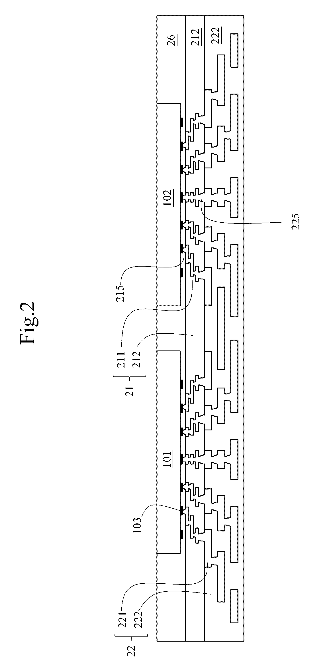
[0018]FIG. 2 shows a system in package (SiP) which comprises chips 101, 102 configured on a top side of the package. Each of the chips 101, 102 has a plurality of I / O pads 103 configured on a bottom side of each chip; molding material 26 wraps the chips 101, 102 at least four lateral sides and a bottom side of the chips.

[0019]A first RDL 21 has a first redistribution circuitry 211 embedded in a first dielectric layer 212. The first redistribution circuitry 211, fabricated according to IC design rule, is configured on a bottom side of the molding material 26. A top end of the first redistribution circuitry 211 is electrically coupled to the I / O pads 103 of the chips through a plurality of first metal vias 215.

[0020]A second RDL 22 has a second redistribution circuitry 221 embedded in a second dielectric layer 222. The second redistribution circuitry 221, fabricated according to PCB design rule, is configured on ...

second embodiment

[0025]FIG. 4 shows a second embodiment according to the present invention.

[0026]FIG. 4 shows a plurality of first gold fingers 251 formed on a bottom side of the second dielectric layer 222. The plurality of the first gold fingers 251 are electrically coupled to the second redistribution circuitry 221. The plurality of the first gold fingers 251 function as I / O contacts for the package system.

[0027]A flexible circuit board 271 can be prepared separately. A plurality of gold fingers 272 corresponding to the plurality of gold fingers 251 are formed on a left end of the flexible circuit board 271. A right end of the flexible circuit board 271 is electrically coupled to a power supply, additional electrical components, or a control system.

third embodiment

[0028]FIG. 5 shows a third embodiment according to the present invention.

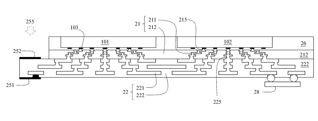
[0029]FIG. 5 shows the second RDL 22 is made wider than the first RDL 21 in the left side. FIG. 5 shows an extended area 255 is formed on a left side of the third RDL 22. A plurality of first gold fingers 251 are formed on a bottom side of the extended area 255. A plurality of second gold fingers 252 are formed on a top side of the extended area 255. The gold fingers 251, 252 are electrically coupled into a gold finger socket (not shown) or other connector (not shown) so that the package can be electrically coupled with additional electronic components. FIG. 6 further shows, at least one passive component 28 such as resistor, capacitor, inductor or other electronic components (not shown) can be optionally configured on a bottom side of the third RDL 23 and electrically coupled to the third redistribution circuitry 231.

[0030]While several embodiments have been described by way of example, it will be apparent to ...


PUM


Abstract

An electronic system without using solder balls between electrical components, and without using interposer between chips and package substrate, without using a discrete system board for the chip package to mount. A chip is wrapped by molding material, a first redistribution circuitry is built on a bottom side of the molding material; a second redistribution circuitry is built on a bottom side of the first redistribution circuitry. A third redistribution circuitry is built on a bottom side of the second redistribution circuitry. Plated metal vias are configured between each two of the electrical components.

Description

BACKGROUND[0001]Technical Field[0002]The present invention relates to an electrical package system; especially relates to a system in package (SiP) without using the following components: discrete solder balls, discrete interposer, discrete package substrate, underfill, and discrete system board.[0003]Description of Related Art[0004]FIG. 1 shows a prior art.[0005]FIG. 1 shows chips 101, 102 configured on a top side of a traditional system in package. Three pluralities of solder balls 141, 142, 143 have been used to join each two components of the system. A first plurality of solder balls 141 join the chips 101, 102 to the silicon interposer 11. A second plurality of solder balls 142 join the silicon interposer 11 to the package substrate 12. A third plurality of solder balls 143 join the package substrate 12 to the system board 13.[0006]Each of the chips 101, 102 has a plurality of I / O pads 103 configured on a bottom side of the chip. The silicon interposer 11 has a core silicon sub...

Claims


Application Information

Patent Timeline
Patent Type & Authority Applications(United States)
IPC IPC(8): H01L23/538H01L23/522H01L21/768H01L23/532H01L25/16H01L23/31H01L21/56
CPCH01L23/5386H01L23/3114H01L23/5226H01L21/768H01L23/53242H01L25/16H01L21/565H01L21/50H01L23/481H01L23/488H01L24/02H01L24/80H01L2224/02379H01L2224/02331H01L2224/80001H01L21/60H01L21/568H01L23/5389H01L24/19H01L24/20H01L2224/04105H01L2224/12105H01L2924/18162H01L2924/19041H01L2924/19042H01L2924/19043H01L24/96H01L23/49805H01L23/49866H01L25/0652H01L25/0655H01L25/50H01L2224/02311H01L2224/02373H01L2224/02381
Inventor HU, DYI-CHUNG
Owner HU DYI CHUNG
Why Eureka
Try Eureka