Electro-optical device, electronic apparatus, and method of driving electro-optical device

a technology of electrooptical devices and electronic devices, applied in the direction of electrical devices, semiconductor devices, instruments, etc., can solve the problems of increasing cost and circuit size, and achieve the effect of ensuring the required capacitance without increasing the size of the circui

Active Publication Date: 2017-05-04
SEIKO EPSON CORP
View PDF1 Cites 10 Cited by
  • Summary
  • Abstract
  • Description
  • Claims
  • Application Information

AI Technical Summary

Benefits of technology

[0008]An advantage of some aspects of the invention is to secur

Problems solved by technology

However, in JP-A-2009-282191, the capacitance element is added to the data line in the outside of t

Method used


Image

  • Electro-optical device, electronic apparatus, and method of driving electro-optical device
  • Electro-optical device, electronic apparatus, and method of driving electro-optical device
  • Electro-optical device, electronic apparatus, and method of driving electro-optical device

Examples


first embodiment

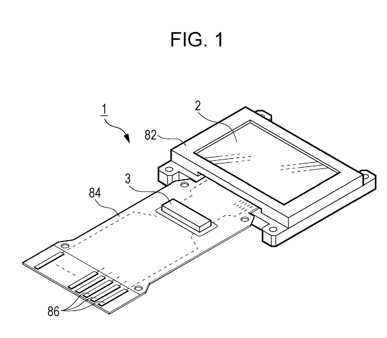
[0052]FIG. 1 is a perspective diagram illustrating a configuration of an electro-optical device 1 according to a first embodiment of the invention. For example, the electro-optical device 1 is a micro display which displays an image in a head-mounted display.

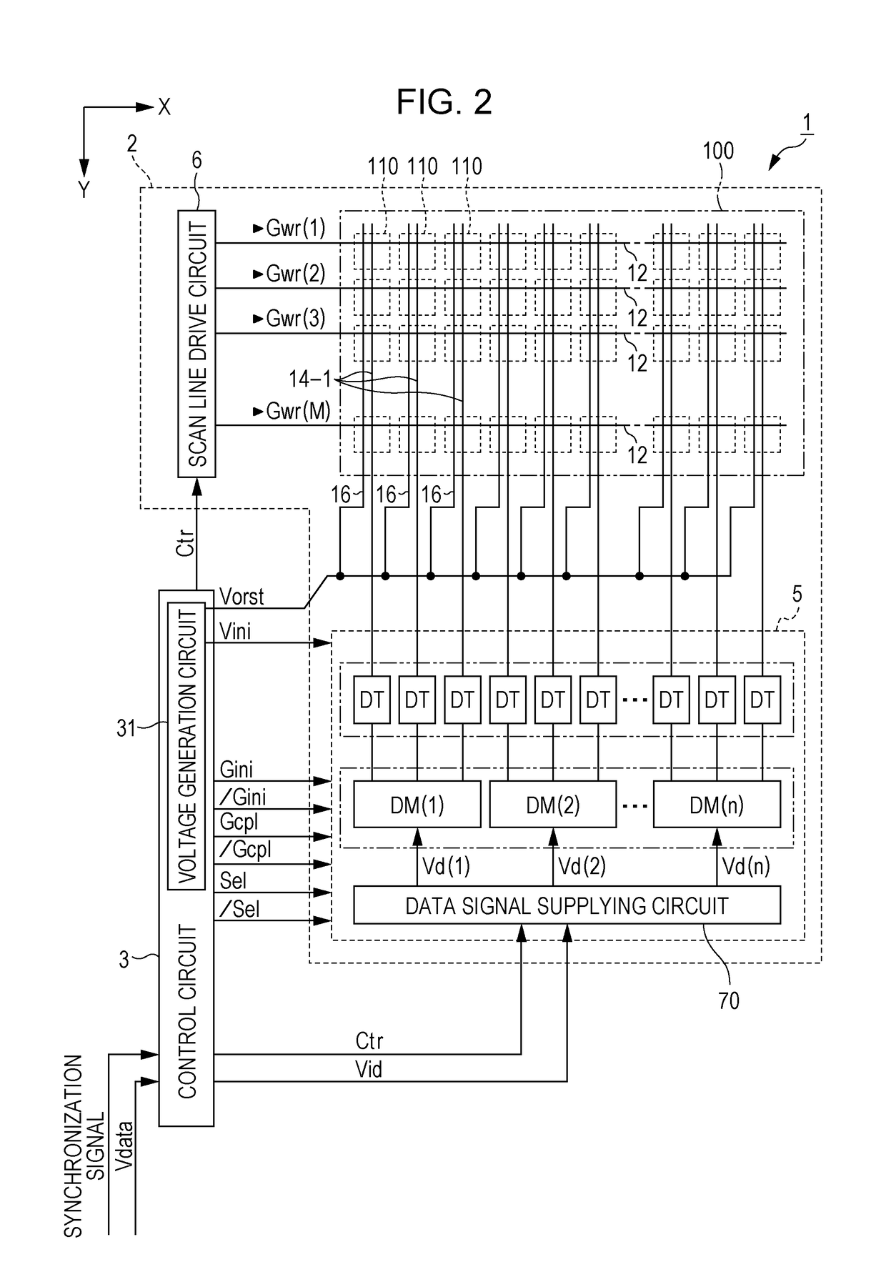
[0053]As illustrated in FIG. 1, the electro-optical device 1 includes a display panel 2, and a control circuit 3 that controls an operation of the display panel 2. The display panel 2 includes a plurality of pixel circuits, and a drive circuit that drives the pixel circuit. In the present embodiment, the plurality of pixel circuits and the drive circuit that are included in the display panel 2 are formed on a silicon substrate, and an OLED that is an example of a light emitting element is used for the pixel circuits. In addition, for example, the display panel 2 is contained in a case 82 of a frame shape that is opened in a display unit, and is coupled to one end of a flexible printed circuit (FPC) substrate 84.

[0054]The control...

second embodiment

[0207]Next, a second embodiment of the invention will be described with reference to FIG. 18 to FIG. 20 of the accompanying drawings. In the second embodiment, the same symbols or reference numerals will be attached to the same members as in the first embodiment.

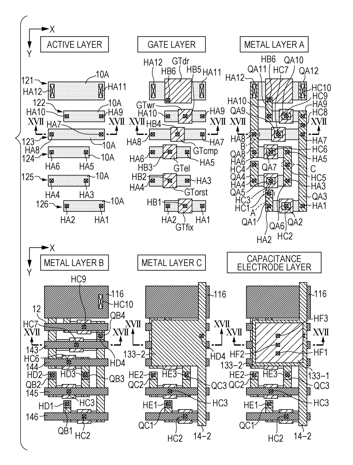
[0208]A circuit according to the present embodiment is the same as the circuit according to the first embodiment illustrated in FIG. 4. In the present embodiment, dispositions of each transistor in a planar view are different from those according to the first embodiment, as illustrated in FIG. 18 to FIG. 20. However, a positional relationship between the respective wires on layers are the same as in the first embodiment.

[0209]As can be understood from FIG. 18 and FIG. 20, also in the present embodiment, the transfer capacitor (first capacitor) 133 is formed of the first electrode 133-1 which is a metal, the insulating layer LD, and the second electrode 133-2 which is a metal, and is configured by a metal-insulator-metal (MIM...

third embodiment

[0227]Next, a third embodiment of the invention will be described with reference to FIG. 23 to FIG. 26 of the accompanying drawings. Six transistors are used in the respective embodiments described above, but five transistors are used in the present embodiment.

Circuit Diagram

[0228]The present embodiment is different from the respective embodiments described above in that a configuration in which the fifth transistor 125 is not included is provided as illustrated in FIG. 23. In addition, a power supplying line 17 to which the initial potential Vini is supplied is coupled to a drain or a source of the first transistor 126. In addition, a voltage Vref which initializes the first data transfer line 14-1 is supplied to the first data transfer line 14-1 through the transmission gate 45. The voltage Vref may be equal to the initial potential Vini.

[0229]An operation according to the present embodiment is the same as that of each embodiment described above, and the second data transfer line ...


PUM


Abstract

An electro-optical device includes a first electrode that is coupled to a first data transfer line, a second electrode that is coupled to a second data transfer line. The first and second electrodes are respectively formed in different layers. A first capacitor is formed of the first electrode, the second electrode, and a dielectric film between the first electrode and the second electrode. In addition, a power supplying line and the first data transfer line are formed in a same layer. A second capacitor is formed of the power supplying line, the first data transfer line, and an insulating layer between the power supplying line and the first data transfer line.

Description

BACKGROUND[0001]1. Technical Field[0002]The present invention relates to an electro-optical device, an electronic apparatus, and a method of driving the electro-optical device.[0003]2. Related Art[0004]In recent years, various electro-optical devices that use a light emitting element such as an organic light emitting diode (hereinafter, referred to as OLED) have been proposed. In a general configuration of the electro-optical device, a pixel circuit that includes a light emitting element, a transistor, or the like is provided in correspondence with a pixel among an image to be displayed, corresponding to intersection of a scan line and a data line.[0005]In the configuration, if a data signal having a potential according to a gradation level of the pixel is applied to a gate of the transistor, the transistor supplies a light emitting element with a current according to a gate-source voltage. According to this, the light emitting element emits light in brightness according to a gradat...

Claims


Application Information

Patent Timeline
IPC IPC(8): H01L27/32G09G3/3233
CPCH01L27/3265H01L27/3276H01L27/3262H01L27/3272G02B2027/0178G09G2300/0819G09G2320/045G02B27/017G09G3/3233G09G3/20G09G2310/0264G09G3/3291G09G2300/0861G09G2310/0251G09G2310/0297G02B2027/0118H10K59/1213H10K59/1216H10K59/131H10K59/126
Inventor OTA, HITOSHINOZAWA, RYOICHI
Owner SEIKO EPSON CORP
Why Eureka
Try Eureka