Optical detection element and solid-state image pickup device
a detection element and solid-state image technology, applied in the direction of diodes, semiconductor devices, radiation controlled devices, etc., can solve the problems of low voltage-sensitivity of early cmos solid-state image pickup devices, and achieve high voltage-sensitivity, radiation tolerance, and radiation tolerance. high
- Summary
- Abstract
- Description
- Claims
- Application Information
AI Technical Summary
Benefits of technology
Problems solved by technology
Method used
Image
Examples
first embodiment
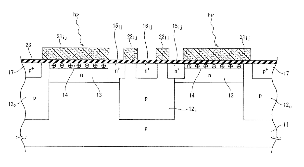
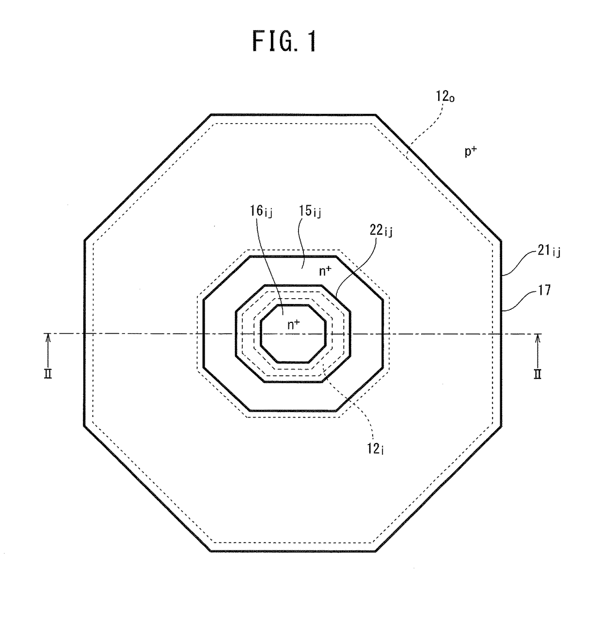
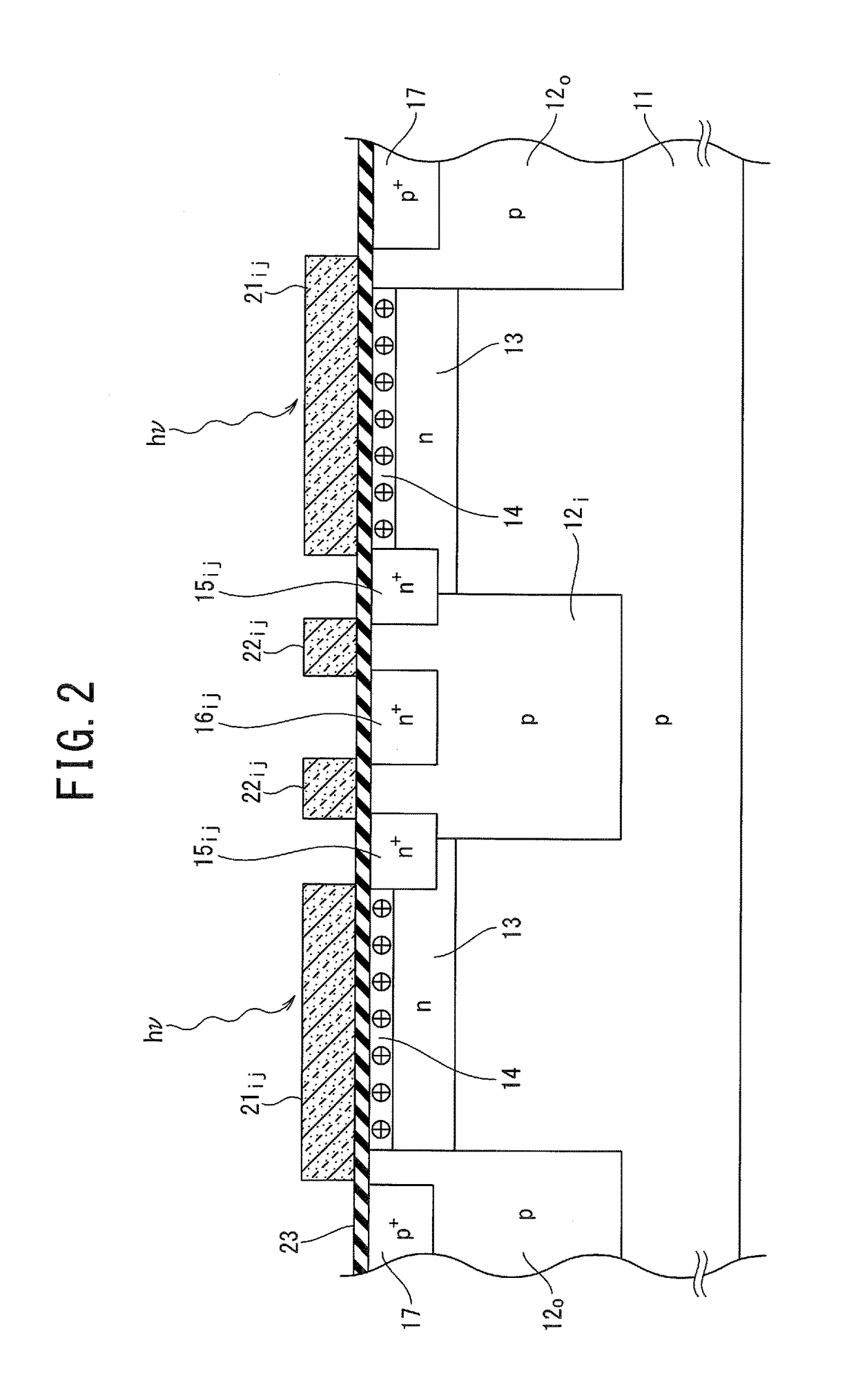
[0029]As illustrated in FIGS. 1 and 2, an optical detection element according to a first embodiment of the present invention includes a base-body region 11 made of a semiconductor having a first conductivity type (p-type), a gate insulating film 23 contacted with an upper surface of the base-body region 11, a buried charge-generation region 13 of a second conductivity type (n-type) buried with an annular form (a ring form in the plan view of FIG. 1) in an upper portion of the base-body region 11 in contact with the gate insulating film 23, a charge-readout region 15i,j of the second conductivity type having a higher impurity concentration than the buried charge-generation region 13, buried with an annular form in an upper portion of the base-body region 11 at a position close to an inner-contour side of the buried charge-generation region 13, a reset-drain region 16i,j of the second conductivity type having a higher impurity concentration than the buried charge-generation region 13,...
second embodiment
[0081]As illustrated in FIGS. 9 and 10, an optical detection element according to a second embodiment of the present invention is the same as the optical detection element according to the first embodiment in that the optical detection element includes a base-body region 11 made of a semiconductor having a first conductivity type (p-type), a gate insulating film 23 contacted with an upper surface of the base-body region 11, a buried charge-generation region 13 of a second conductivity type (n-type) buried with an annular form (a ring form in the plan view of FIG. 9) in an upper portion of the base-body region 11 in contact with the gate insulating film 23, a charge-readout region 15i,j of the second conductivity type having a high impurity concentration than the buried charge-generation region 13, buried with an annular form in an upper portion of the base-body region 11 at a position close to an inner-contour side of the buried charge-generation region 13, a reset-drain region 16i,...
PUM
 Abstract
Description
Claims
Application Information


