
Voltage calibration method for electro-optical detector

A voltage calibration and detector technology is applied in the field of calibrating the modulation signal voltage of an electro-optical detector to achieve practical results.

Inactive Publication Date: 2011-06-22
JILIN UNIV
View PDF0 Cites 0 Cited by
  • Summary
  • Abstract
  • Description
  • Claims
  • Application Information

AI Technical Summary

Problems solved by technology

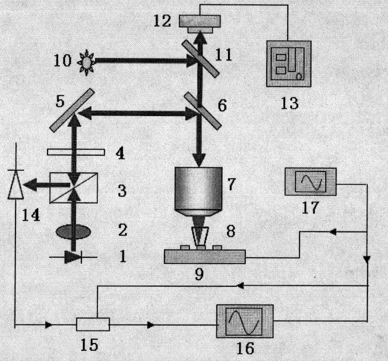
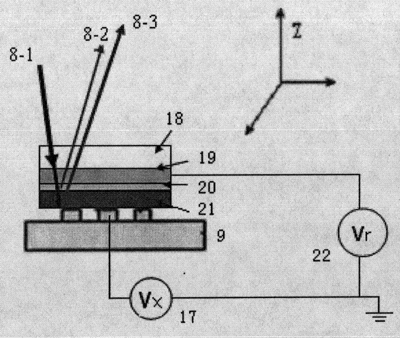
[0005] The invention introduces a standard signal with a known voltage amplitude through the reference electrode 19 to realize voltage calibration, which solves the practical problem of electro-optic detection

Method used


Image

  • Voltage calibration method for electro-optical detector
  • Voltage calibration method for electro-optical detector
  • Voltage calibration method for electro-optical detector

Examples


Embodiment 1

[0070] Example 1: Making a coplanar waveguide circuit with a uniform surface electric field as a measurement and research object

[0071] Firstly, a 1 μm thick gold film is vapor-deposited on an optically polished transparent substrate (such as glass), and then photolithographically produced as Figure 5 (a) Waveguide circuit with regular structure shown. The transmission line in the coplanar waveguide circuit is equivalent to the transmission line on the integrated circuit chip, so it can replace the integrated circuit chip as the measurement object of the experiment.

[0072] The voltage of the transmission line on the coplanar waveguide circuit 23 is measured by the aforementioned piezoelectric calibration method, and the distance between any position on the transmission line and the surrounding waveguide circuit is the same, so the electric field distribution is the same.

[0073] Using the electro-optic sampling device of the present invention, 8 points are taken at diff...

Embodiment 2

[0077] Example 2: Making a coplanar waveguide circuit with uneven surface electric field distribution as a measurement and research object

[0078] As shown in 6(a), the distance between each point on the transmission line of the coplanar waveguide circuit 24 and the adjacent ground line is different, so that the force distribution of the power line is different, resulting in a difference between the amplitude of the electric field signal and the amplitude of the induced electro-optical modulation signal The corresponding relationship is uncertain, but in formula (7), the measured and calculated value has nothing to do with the spacing of the waveguide, so the accurate voltage value of each point on the waveguide can also be accurately measured and calculated.

[0079] Adopt the method for utilizing the reference voltage of the above-mentioned invention, measure the measurement result as table 2, the measurement result on the same wire is the same within the error range.

[00...

Embodiment 3

[0082] Embodiment 3: Making a coplanar waveguide circuit with surface electric field gradient distribution as a measurement and research object

[0083] As shown in 6(b), the coplanar waveguide circuit 25 is a circuit using three 2k ohm resistors to divide the voltage. The voltage calibration method of the present invention is used to measure the voltages on the three transmission lines. The measured data are shown in Table 3. The actual measurement The result 1.66:1.125:0.6≈3:2:1 conforms to the principle of partial pressure.

[0084] Table 3: Measured data of coplanar waveguide voltage divider circuit

[0085]

[0086] In summary, all measured and calculated values ​​are consistent with the actual voltage values. Voltage signals on different measurement points on the same transmission line, transmission lines with different spacings and transmission lines that have been divided by resistance can be accurately calibrated. The measurement results prove that it is f...


PUM


Abstract

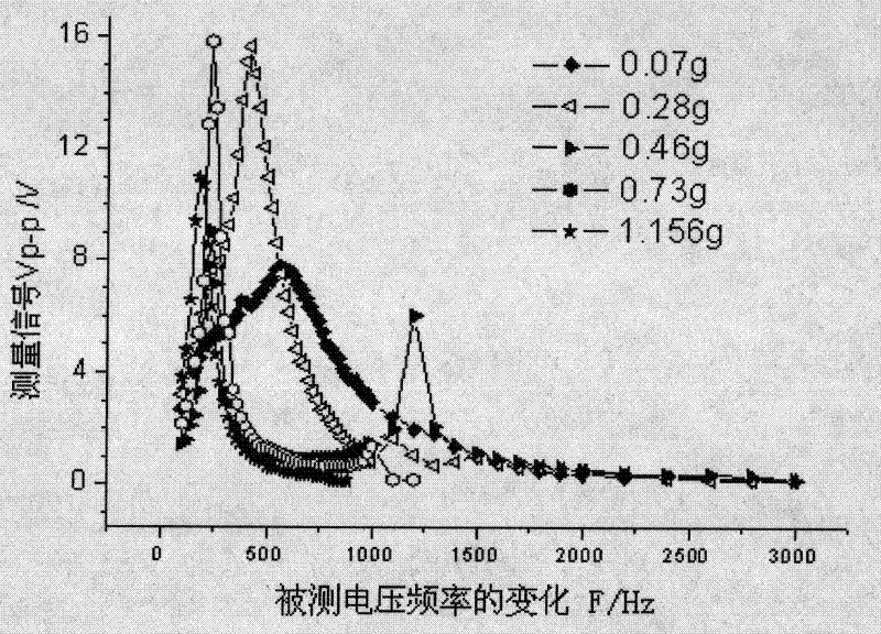
The invention belongs to the field of electro-optical sampling technique of an integrated circuit, and more particularly relates to a method for calibrating modulating signal voltage of an electro-optical detector. The method is a new technique for calibrating the measured voltage near the DC area (within 10MHz) when in fault diagnosis for the integrated circuit. Voltage calibration measurement is always the problem to be solved in the electro-optic detection technology. The method utilizes piezoelectric harmonic peak of electro-optic material in low frequency area near DC, so that the voltage sensitivity of electro-optic detection can be increased by two orders of magnitude. The upper surface of an electro-optic dielectric layer of a probe is introduced with a reference electrode which is accessed with an electrical signal that have the same frequency as that of the measured circuit, are the same as or opposite to the measured voltage signal and has the known voltage amplitude, and the electrical signal is taken as the standard of comparison, so that the calibration for the measured voltage amplitude can be realized, the average measurement error is less than 6%, and the demand of fault diagnosis for the integrated circuit can be met.

Description

technical field [0001] The invention belongs to the technical field of integrated circuit electro-optic sampling, and in particular relates to a method for calibrating the modulation signal voltage of an electro-optic detector. Background technique [0002] With the development of microelectronic chip manufacturing technology, the integration and operation speed of chips are getting higher and higher. In order to improve the design and manufacturing process of integrated circuits and improve the reliability of integrated circuits, it is necessary to detect and analyze faulty integrated circuit chips. Electro-optical detection is a method of non-destructive detection of the internal voltage characteristics of the chip by optical methods. The voltage sensitivity and the spatial resolution of 0.5μm have always been a topic of concern in the field of microelectronics reliability research. [0003] Due to problems such as parasitic capacitance and distribution parameter unce...

Claims


Application Information

Patent Timeline
Patent Type & Authority Patents(China)
IPC IPC(8): G01R35/00G01R31/311
Inventor 孙洪波金如龙衣茂斌杨罕赵迪
Owner JILIN UNIV
Learn More