Mems piezoelectric vector hydrophone with series structure and preparation method thereof
A technology of vector hydrophone and series structure, which is applied in the field of sensing, can solve the problems of low sensitivity, poor temperature stability, and easy adhesion of devices, etc., and achieve the effect of improved sensitivity and simple preparation process
- Summary
- Abstract
- Description
- Claims
- Application Information
AI Technical Summary
Problems solved by technology
Method used
Image
Examples
Embodiment 1
[0040] 1) Clean the substrate
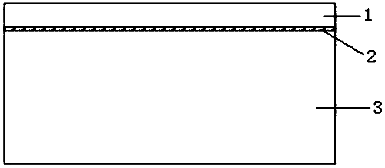
[0041] Clean the SOI silicon wafer with a standard cleaning method, first use acidic cleaning solution and alkaline cleaning solution to boil and clean, then clean with deionized water, and finally blow dry with nitrogen. figure 2 It is a cross-sectional view of the substrate SOI silicon wafer of the chip, such as figure 2 As shown, the SOI silicon wafer includes: SOI base layer 3 , SOI oxide layer 2 and SOI silicon layer 1 . The SOI base layer 3 has a thickness of 500 μm, the SOI oxide layer 2 has a thickness of 0.05 μm, and the SOI silicon layer 1 has a thickness of 10 μm.
[0042]2) deposit insulating oxide layer 4
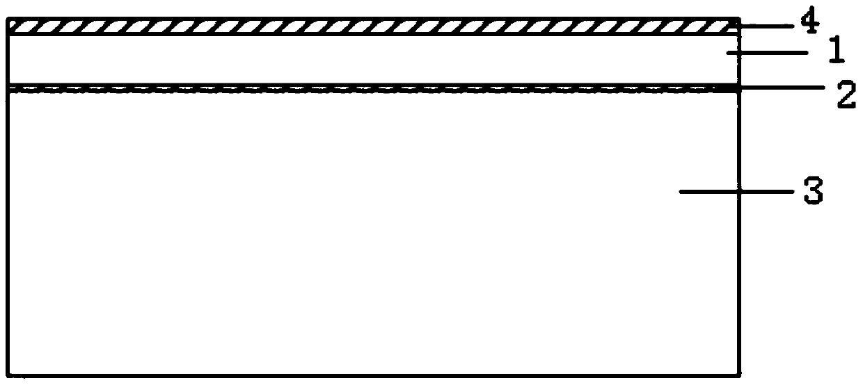
[0043] The insulating oxide layer 4 is formed on the surface of the substrate by thermal oxidation furnace, and the profile of the chip after the insulating oxide layer is deposited on the front side is as follows: image 3 As shown, wherein, after depositing an insulating oxide layer 4 with a thickness of 1 μm, the front si...
Embodiment 2
[0070] 1) Clean the substrate
[0071] Clean the SOI silicon wafer with a standard cleaning method, first use acidic cleaning solution and alkaline cleaning solution to boil and clean, then clean with deionized water, and finally blow dry with nitrogen. The SOI silicon wafer includes: the thickness of the SOI base layer 3 is 300 μm, the thickness of the SOI oxide layer 2 is 0.5 μm, and the thickness of the SOI silicon layer 1 is 1 μm, such as figure 2 shown.
[0072] 2) deposit insulating oxide layer 4
[0073] Utilize thermal oxidation furnace to form insulating oxide layer 4 on substrate surface oxidation, as image 3 As shown, the thickness is 20 μm, the front side is protected by photoresist immediately, and the silicon dioxide on the back side is etched with a slow-release hydrofluoric acid (BHF) solution to remove the photoresist.
[0074] 3) Etching mask for back deposit
[0075] A 0.01 μm silicon nitride film 5 is deposited on the back of the silicon wafer by plas...
Embodiment 3
[0093] 1) Clean the substrate
[0094] Clean the SOI silicon wafer with a standard cleaning method, first use acidic cleaning solution and alkaline cleaning solution to boil and clean, then clean with deionized water, and finally blow dry with nitrogen. The SOI silicon wafer includes: the thickness of the SOI base layer 3 is 400 μm, the thickness of the SOI oxide layer 2 is 1 μm, and the thickness of the SOI silicon layer 1 is 0.5 μm, such as figure 2 shown.
[0095] 2) deposit insulating oxide layer 4
[0096] Utilize thermal oxidation furnace to form insulating oxide layer 4 on substrate surface oxidation, as image 3 As shown, the thickness is 10 μm, the front side is protected by photoresist immediately, and the back side silicon dioxide is etched with a slow-release hydrofluoric acid (BHF) solution to remove the photoresist.
[0097] 3) Etching mask for back deposit
[0098] A 1 μm silicon oxide film 5 is deposited on the back of the silicon wafer by plasma enhanced ...
PUM
 Abstract
Description
Claims
Application Information


