

Electro-optical detector capable of calibrating voltage
A technology for calibrating voltages and detectors, used in electronic circuit testing, measuring current/voltage, instruments, etc., and can solve problems such as non-uniformity
- Summary
- Abstract
- Description
- Claims
- Application Information
AI Technical Summary
Problems solved by technology
Method used
Image

Examples
Embodiment 1
[0026] Embodiment 1 The structure and working principle of the electro-optical probe of the present invention
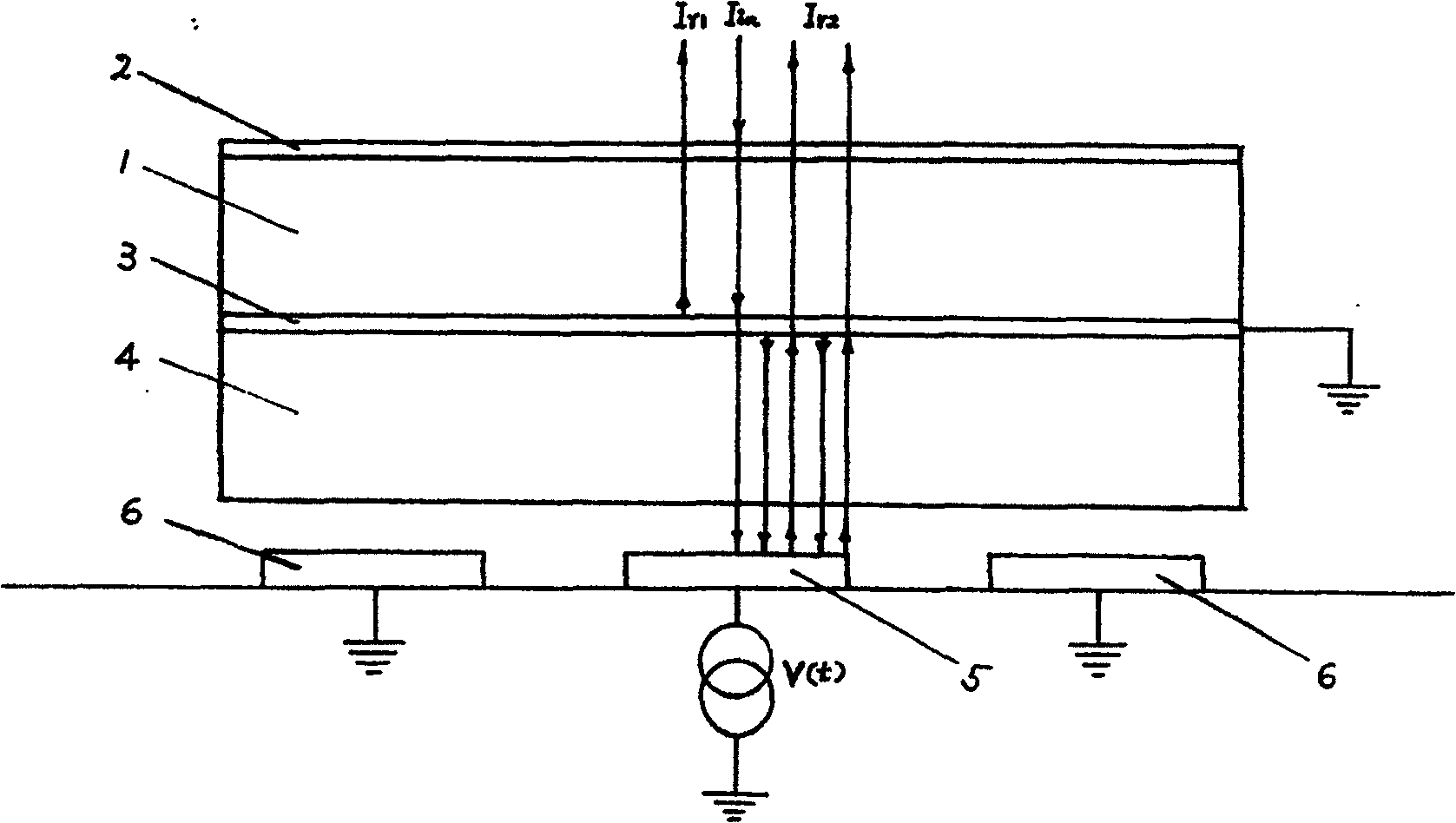
[0027] The structure of the electro-optical probe of the present invention is as image 3 shown. The transparent substrate 1 can be transparent silicon oxide glass or a transparent crystal that has no birefringence effect on the probe light. A layer of anti-reflection film 2 is coated on the upper surface of the transparent substrate 1, and a layer of grounded conductive film 3 with selective reflection characteristics is coated on the lower surface of the transparent substrate 1. The conductive film has a reflectivity r of about 0.35 for the wavelength of the probe light. 1 and a transmittance t around 0.65 1 . reflectivity r 1 and transmittance t 1 The optimal selection of the specific value of the measured circuit is related to the reflectivity r of the metal microstrip line 5 for the transmission of the electrical signal to the probe light 2 Associated. i...
Embodiment 2
[0033] Embodiment 2 Electro-optical detection optical unit structure used in conjunction with the electro-optic probe of the present invention
[0034] The electro-optical detection optical unit used in conjunction with the electro-optic probe of the present invention is as Figure 4 shown. Wherein, 7 is the driving device of the laser. If electro-optic sampling measurement is to be done, the driving device 7 of the laser should be a microwave signal generator, and the microwave power of its output drives the laser device 8 to generate a gain switch ultrashort pulse beam; if the electro-optic measurement of continuous light is to be done, the driving device 7 of the laser Should be a DC power supply. The laser 8 may be a laser diode, which generates near-infrared light of any wavelength within the range of 1.25 microns to 1.3 microns as probe light. The detection beam is transformed into parallel light by the collimator lens 9, its polarization direction is determined by th...
Embodiment 3
[0038] The preparation of embodiment 3 electro-optical medium layer
[0039] The electro-optic medium layer 4 can be any electro-optic material film with rotational axis symmetry, and a convenient and applicable material is a non-linear optical material film prepared by sol-gel method.
[0040] Dissolve the appropriate proportion of chromophores and crosslinking agent materials in the same solvent to form a sol, and evenly spin-coat the sol on the grounded conductive film 3 of the transparent substrate 1, and perform corona polarization and heat curing on the formed dielectric film Processing, that is to obtain a polarized polymer film with electro-optic effect, the polarization direction is the normal direction of the grounding conductive film 3, and also the direction of the rotational symmetry axis of the film material, and the thickness of the film requires that when the electro-optic probe 14 contacts the electric signal transmission line The vertical distance from the me...
PUM
 Abstract
Description
Claims
Application Information