OLED display device
- Summary
- Abstract
- Description
- Claims
- Application Information
AI Technical Summary
Benefits of technology
Problems solved by technology
Method used
Image
Examples
first embodiment
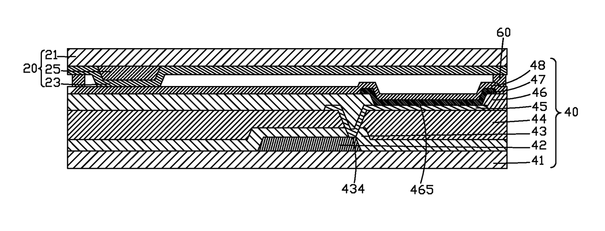
[0049]Referring to FIG. 2, the OLED display device according to the present invention is shown. In the instant embodiment, the upper substrate 20 further comprises a first photo spacer 25 arranged on the first base plate 21. The first photo spacer 25 is a protrusion formed on the first base plate 21 and is not electrically conductive. The assisting conductive layer 23 is arranged on the first photo spacer 25 and the first base plate 21 and covers the first photo spacer 25, wherein a portion of the assisting conductive layer 23 that covers the first photo spacer 25 is set in direct contact with the second electrode 48 that is arranged on a top surface of the lower substrate 40 so that electrical connection between the second electrode 48 and the assisting conductive layer 23 is achieved.
second embodiment
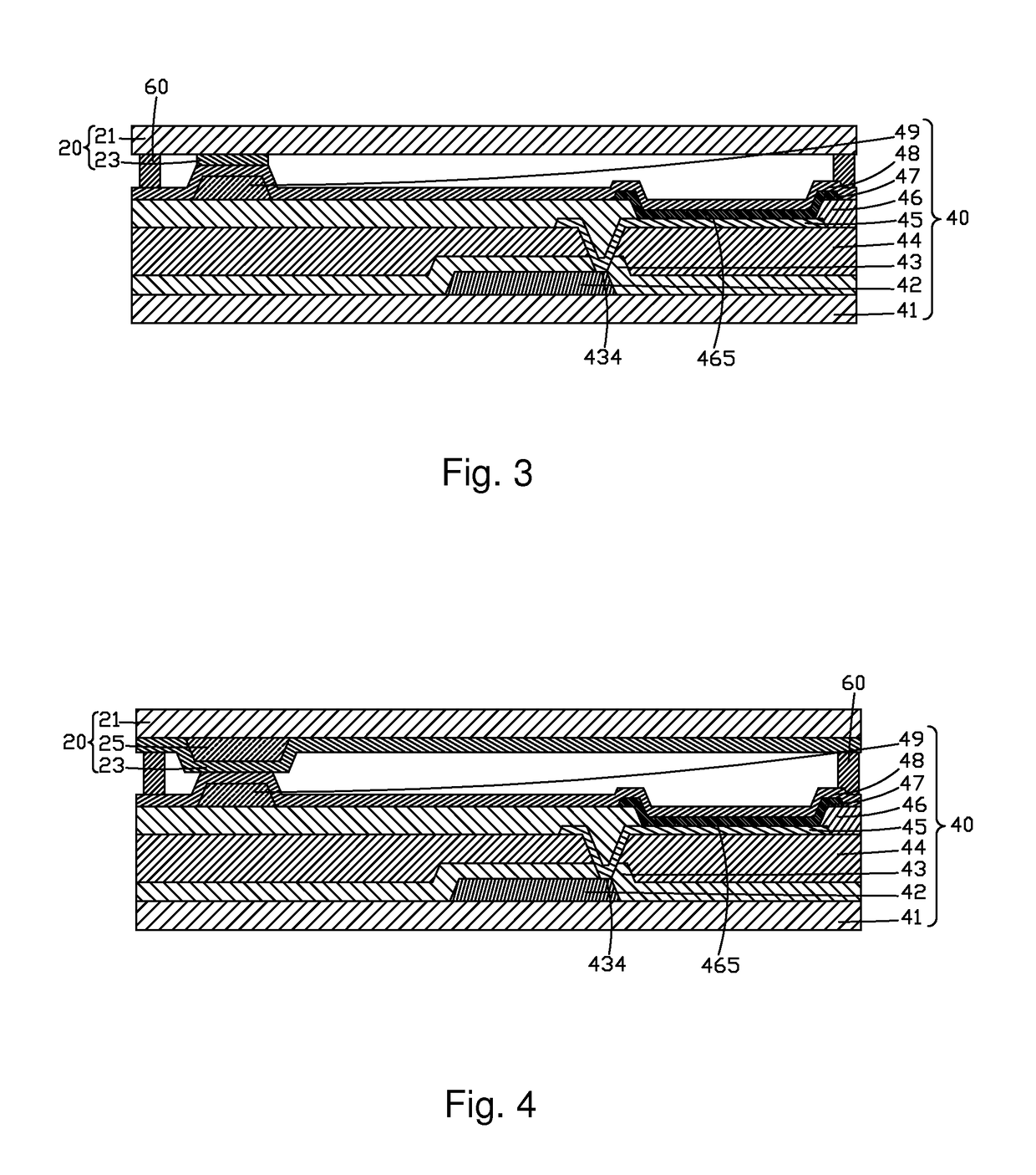
[0050]Referring to FIG. 3, the OLED display device according to the present invention is shown. In the instant embodiment, the lower substrate 40 further comprises a second photo spacer 49 arranged on the pixel definition layer 46. The second photo spacer 49 is a protrusion formed on the first base plate 21 and is not electrically conductive. The second electrode 48 is arranged on the second photo spacer 49, the pixel definition layer 46, and the OLED light emission layer 47 and covers the second photo spacer 49, wherein a portion of the second electrode 48 that covers the second photo spacer 49 is set in direct contact with the assisting conductive layer 23 that is arranged on a bottom surface of the upper substrate 20 so that electrical connection between the second electrode 48 and the assisting conductive layer 23 is achieved.
third embodiment
[0051]Referring to FIG. 4, the OLED display device according to the present invention is shown. In the instant embodiment, the upper substrate 20 further comprises a first photo spacer 25 arranged on the first base plate 21 and the assisting conductive layer 23 is arranged on the first photo spacer 25 and the first base plate 21 and covers the first photo spacer 25; the lower substrate 40 further comprises a second photo spacer 49 arranged on the pixel definition layer 46 and the second electrode 48 is arranged on the second photo spacer 49, the pixel definition layer 46, and the OLED light emission layer 47 and covers the second photo spacer 49, wherein the first photo spacer 25 of the upper substrate 20 and the second photo spacer 49 of the lower substrate 40 are arranged to correspond to each other and a portion of the assisting conductive layer 23 that covers the first photo spacer 25 is set in direct contact with a portion of the second electrode 48 that covers the second photo...
PUM
 Abstract
Description
Claims
Application Information


