Flat Lighting Devices and Method of Contacting Flat Lighting Devices

Inactive Publication Date: 2009-12-10
FRAUNHOFER GESELLSCHAFT ZUR FOERDERUNG DER ANGEWANDTEN FORSCHUNG EV
View PDF5 Cites 25 Cited by
  • Summary
  • Abstract
  • Description
  • Claims
  • Application Information

AI Technical Summary

Benefits of technology

[0019]Thus, in embodiments, the contact regions (anode contact region and cathode contact region) are arranged symmetrically along the edge so as to ensure connection which is protected against polarity inversion upon rotation of the plate (flat lighting device). In addition, the share of the sizes of the contact areas (circulation length) is proportional to the layer resistance ratio between the anode and cathode layers. In further embodiments, an additional central contact is also formed which further increases the homogeneity of the supply of current. For example, a central contact for the cathode may be formed in that the anode contact region is centrally interrupted, for example, and in that a cathode contact region is formed there. To continue to ensure connection which is protected from polarity inversion, said centr

Problems solved by technology

Due to the low conductivity of the TCO layer, said layers frequently limit the homogeneity of the current density distribution as well as the maximally achievable size of a lighting area.
With large-area lighting elements, the high-impedance resistance of the ITO layer results in an inhomogeneity of the supply of current.
Due to the non-transparency of these metal grids, however, the effective lighting area is reduced accordingly.
A useful improvement would be an increase in the grid metal thickness, for example, which, however, is not practical because of the structuring, or patterning, possibilities and the layer thicknesses of the organic layers.
Additionally, an ITO layer reinforced by metal is contacted only on the outer edges, which limits the maximum surface area of a lighting element despite the effective reduction in resistance.
This does not resul

Method used


Image

  • Flat Lighting Devices and Method of Contacting Flat Lighting Devices
  • Flat Lighting Devices and Method of Contacting Flat Lighting Devices
  • Flat Lighting Devices and Method of Contacting Flat Lighting Devices

Examples


Embodiment Construction

[0042]Before discussing the present invention in more detail below with reference to the drawings, it shall be noted that identical elements in the figures are designated by identical or similar reference numerals, and that repeated descriptions of said elements have been omitted.

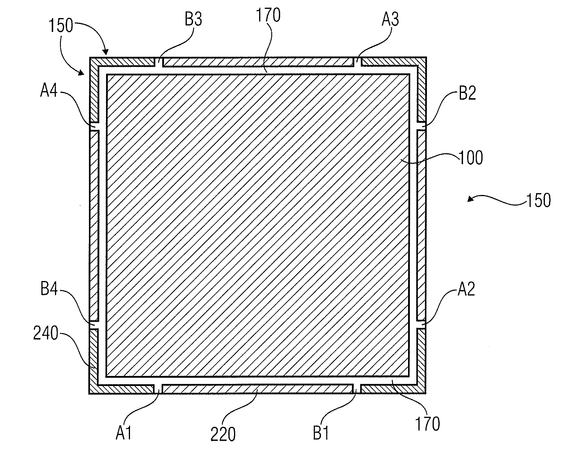
[0043]FIG. 1 shows a schematic top view of a flat lighting device having a layer arrangement 100 which comprises a flat shape and is limited by an edge 150, which may also be implemented as an edge region. In this embodiment, the flat shape is implemented as a square, so that there is a rotational invariance toward rotations by an angle α=90°. In addition, the flat lighting device comprises an anode contact region 220 and a cathode contact region 240, the anode and cathode contact regions 220, 240 being implemented along the edge 150 and contacting the layer arrangement 100.

[0044]In the embodiment shown in FIG. 1, the cathode contact regions 240 are implemented at the corner points of the square shape of th...


PUM


Abstract

A flat lighting device includes a layer arrangement, anode and cathode contact regions. The layer arrangement includes an anode layer, a cathode layer, and an organic light-emitting layer arranged between the anode and cathode layers, the layer arrangement having a flat shape which is laterally bounded by an edge region. The anode contact regions contact the anode layer and are implemented along the edge region. The cathode contact regions contact the cathode layer and are implemented along the edge region. The flat shape has a rotational invariance toward rotation by discrete angles. The anode and cathode contact regions may be contacted from one side of the flat shape of the layer arrangement and are arranged to be laterally distributed over the edge region such that the lateral distribution of the anode and cathode contact regions is maintained upon rotation of the layer arrangement by the discrete angles.

Description

CROSS-REFERENCE TO RELATED APPLICATIONS[0001]This application claims priority from German Patent Application No. 102008027519.0, which was filed on Jun. 10, 2008, and is incorporated herein in its entirety by reference.[0002]The present invention relates to flat lighting devices and a method of contacting flat lighting devices, and in particular to side contact structures for large-area OLED (organic light-emitting diode) lighting areas.BACKGROUND OF THE INVENTION[0003]Novel area lighting elements may be realized on the basis of organic light-emitting diodes. As flat lighting device, which have moderate luminance as compared to conventional LEDs (light-emitting diodes), OLEDs are ideally suited for producing flat diffuse light sources (e.g. lighting panels). These light sources will be applicable in as manifold a manner as the displays which are based on organic light-emitting diodes. Due to the thin-film technology used, it will further become possible in the production of OLEDs to...

Claims


Application Information

Patent Timeline
IPC IPC(8): H01L51/52H01L21/02F21K99/00
CPCF21S2/005F21Y2105/008H01L27/3202H01L27/3204H01L27/3293H01L2251/5361H01L51/5206H01L51/5212H01L51/5221H01L51/5228H01L51/5203F21Y2105/00F21Y2115/15H10K59/84H10K59/86H10K59/18H10K50/813H10K50/814H10K50/824H10K50/805
Inventor AMELUNG, JOERGKIRCHHOF, CHRISTIANHESSE, JANHOFFMANN, MICHAEL
Owner FRAUNHOFER GESELLSCHAFT ZUR FOERDERUNG DER ANGEWANDTEN FORSCHUNG EV
Why Eureka
Try Eureka