Diode device and manufacturing method thereof

a technology of diodes and diodes, which is applied in the direction of semiconductor devices, basic electric elements, electrical apparatus, etc., can solve the problems of block reverse bias current, high current and super-high speed, and large current leakage of schottky diodes under reverse bias, so as to reduce the reverse current leakage of schottky diodes, reduce the turn on voltage of schottky diodes, and increase the reverse breakdown voltage of scho

Active Publication Date: 2017-05-25
DIODES TAIWAN S A R L
View PDF8 Cites 13 Cited by
  • Summary
  • Abstract
  • Description
  • Claims
  • Application Information

AI Technical Summary

Benefits of technology

[0007]The instant disclosure provides a diode device and manufacturing method thereof for increasing the reverse breakdown voltage of the Schottky diode and reducing the reverse current leakage of the Schottky diode. By increasing the reverse breakdown voltage of the Schottky diode, it can employ Schottky metals with lower barrier and hence, is able to further decrease the turn on voltage of the Schottky diode.

Problems solved by technology

In addition, a Schottky diode may afford larger forward current and may block reverse bias current.
Therefore, Schottky diodes are semiconductor elements with low power, high current and super-high speed.
However, since the reverse breakdown voltage of the Schottky diode is low, the Schottky diode has larger current leakage under reverse bias.
When the reverse bias is larger than the reverse breakdown voltage of the Schottky diode, the reverse current will pass through the Schottky diode and may increase the temperature thereof and lead to a thermal instability issue.
In addition, since the complication of the manufacturing process of the Schottky diode is high, the Schottky diode has a high manufacturing cost.

Method used


Image

  • Diode device and manufacturing method thereof
  • Diode device and manufacturing method thereof
  • Diode device and manufacturing method thereof

Examples


Embodiment Construction

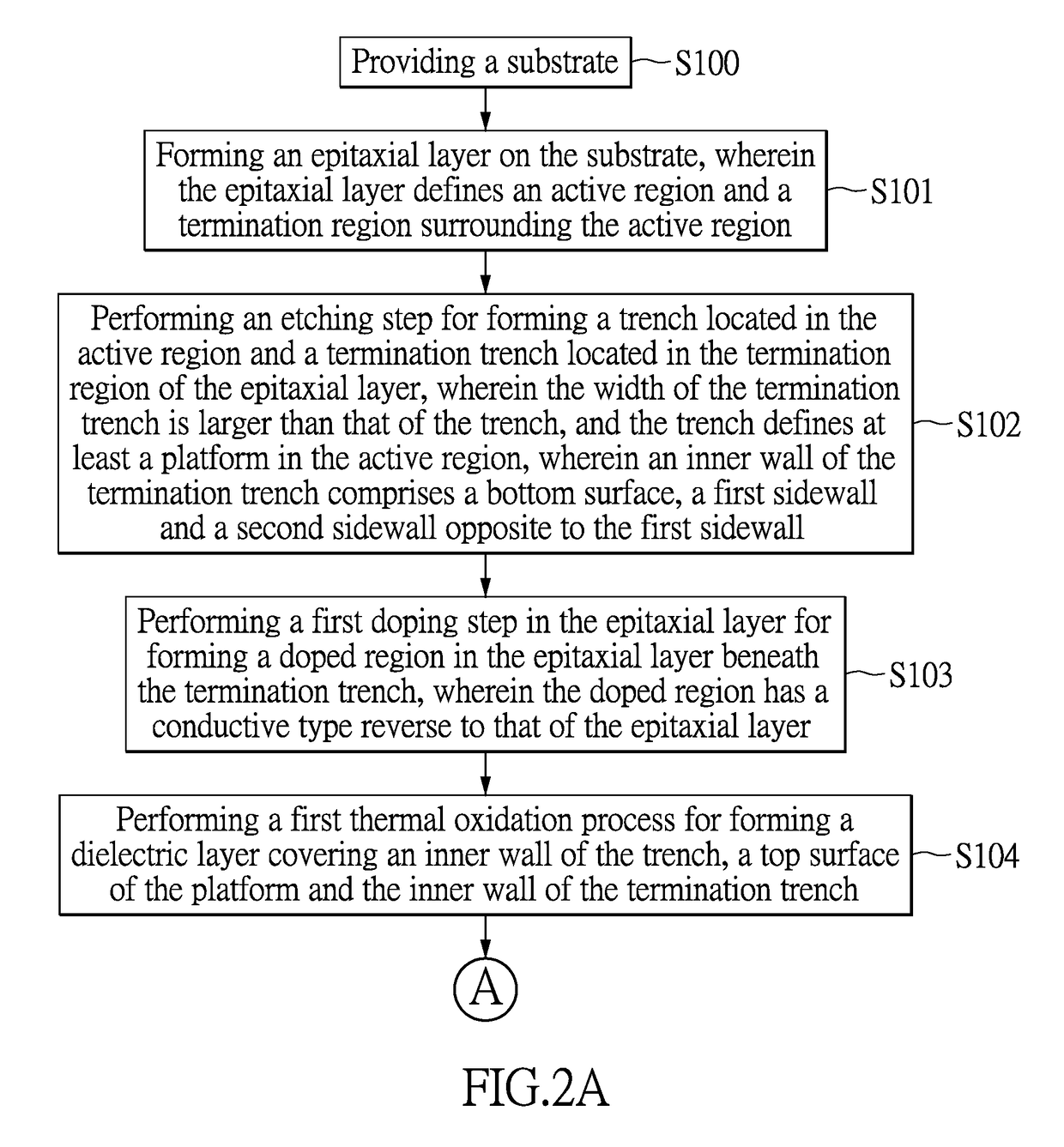
[0017]Reference will now be made in detail to the exemplary embodiments of the instant disclosure, examples of which are illustrated in the accompanying drawings. Wherever possible, the same reference numbers are used in the drawings and the description to refer to the same or like parts.

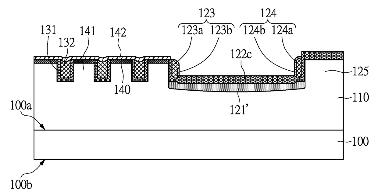
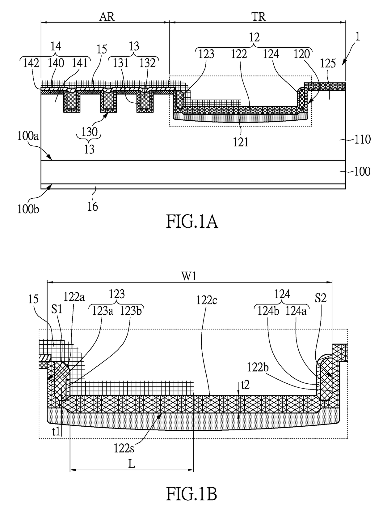
[0018]FIG. 1A is a sectional schematic view of the diode device of an embodiment of the instant disclosure. The diode device 1 of the embodiment of the instant disclosure comprises a substrate 100, an epitaxial layer 110, a termination structure 12, a trench gate electrode structure 13, a Schottky diode structure 14, a first contact pad 15 and a second contact pad 16.

[0019]As shown in FIG. 1A, the substrate 100 is a semiconductor substrate and has a high concentration of a first type conductive dopant, thereby forming a first heavily doped region. The first heavy doped region may be distributed in a partial region of the substrate 100, or the entire substrate 100. The instant disclosure is not limit...


PUM

PropertyMeasurementUnit
depthaaaaaaaaaa
depthaaaaaaaaaa
overlapping lengthaaaaaaaaaa

Abstract

A diode device and manufacturing method thereof are provided. The diode device includes a substrate, an epitaxial layer, a trench gate structure, a Schottky diode structure and a termination structure. An active region and a termination region are defined in the epitaxial layer. The Schottky diode structure and the trench gate structure are located in the active region and the termination structure is located in the termination region. The termination structure includes a termination trench formed in the epitaxial layer, a termination insulating layer, a first spacer, a second spacer and a first doped region. The termination insulating layer is conformingly formed on inner walls of the termination trench. The first and second spacers are disposed on two sidewalls of the termination trench. The first doped region formed beneath the termination trench has a conductive type reverse to that of the epitaxial layer.

Description

BACKGROUND[0001]1. Technical Field[0002]The instant disclosure relates to a diode device and manufacturing method thereof, in particular, to a trench Schottky diode device for rectification and manufacturing method thereof.[0003]2. Description of Related Art[0004]Different from common PN diodes, Schottky diodes utilize the Schottky barrier generated during the bonding of metals and semiconductors, thereby providing the function of rectification. A Schottky diode has a low forward voltage drop and a very fast switching action. In addition, a Schottky diode may afford larger forward current and may block reverse bias current. Therefore, Schottky diodes are semiconductor elements with low power, high current and super-high speed.[0005]Accordingly, Schottky diodes are an important power element and are widely used as output rectifying diodes in switches of power supplies, motor controllers, switches of communication elements, automatic equipment in factories, electronic automatic applic...

Claims


Application Information

Patent Timeline
Patent Type & Authority Applications(United States)
IPC IPC(8): H01L29/872H01L21/265H01L29/06H01L29/66H01L29/47
CPCH01L29/872H01L29/66143H01L21/265H01L29/0619H01L29/47H01L29/8725H01L29/0661
Inventor YU, SHIH-HANTSAI, SUNG-YINGCHANG, YU-HUNGCHUANG, JU-HSUHSU, CHIH-WEI
Owner DIODES TAIWAN S A R L
Why Eureka
Try Eureka