Method for forming insulating layer, method for producing electronic device, and electronic device

a technology of insulating layer and insulating layer, which is applied in the direction of dielectric characteristics, conductive pattern formation, instruments, etc., can solve the problem of high possibility of poor conduction and achieve the effect of preventing poor conduction

Active Publication Date: 2017-06-01
JAPAN AVIATION ELECTRONICS IND LTD
View PDF1 Cites 8 Cited by
  • Summary
  • Abstract
  • Description
  • Claims
  • Application Information

AI Technical Summary

Benefits of technology

[0016]According to this invention, since a wiring pattern in a non-printing region has a characteristic shape, even when an insulating layer covering the wiring pattern is formed by flexographic printing or inkjet printing in such a way that a contact region of the wiring pattern which is used for electrical connection with a conductor other than the wiring pattern is exposed, insulating ink forming the insulating layer by printing does not reach the contact region by moving on a wiring line. This makes it possible to prevent poor conduction from occurring in the contact region.

Problems solved by technology

As a result, there is a high possibility of the occurrence of poor conduction.

Method used


Image

  • Method for forming insulating layer, method for producing electronic device, and electronic device
  • Method for forming insulating layer, method for producing electronic device, and electronic device
  • Method for forming insulating layer, method for producing electronic device, and electronic device

Examples


Embodiment Construction

[0043]The brief overview of this invention is as follows (see FIG. 9).

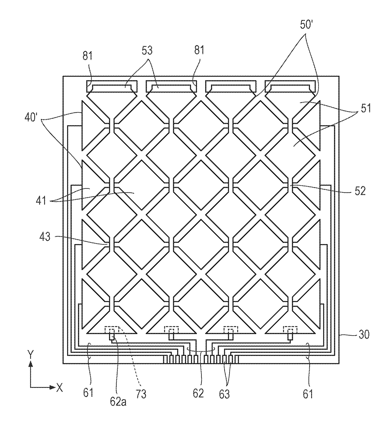
[0044]A wiring pattern is formed on a base by using a conductor film (Step 51).

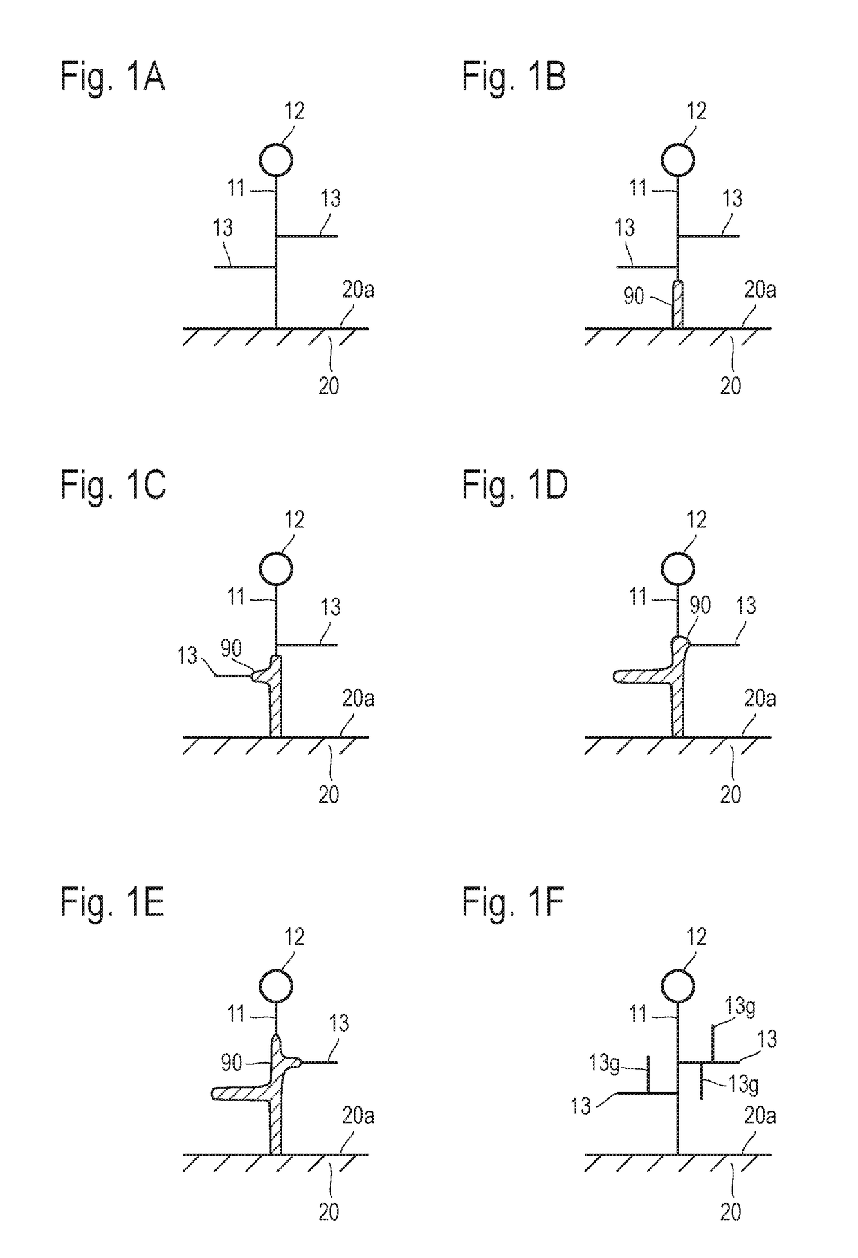
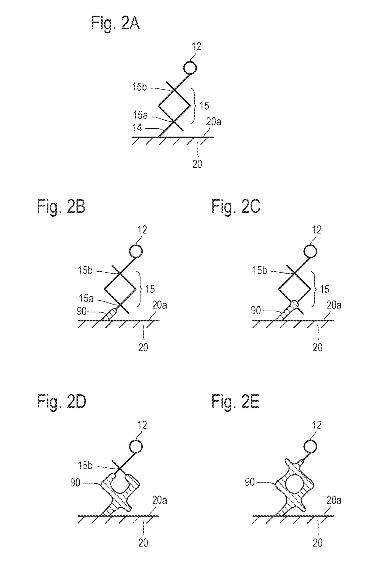
[0045]The wiring pattern is covered with an insulating layer in such a way that a contact region is exposed. The contact region is a region that belongs to the wiring pattern and is used for electrical connection with a conductor other than the wiring pattern. Specifically, insulating ink is applied on the wiring pattern by flexoaraphic printing or inkjet printing in accordance with a printing pattern delimited by an outline of a non-covered region which is a region that includes the contact region therein and is not covered with the insulating layer (Step S2).

[0046]A structure that effectively increases the amount of retained ink without increasing electric resistance is provided somewhere on a wiring line leading, to the contact region, from a position on the wiring pattern at which the wiring pattern overlaps with the outline.

[0047]T...


PUM

PropertyMeasurementUnit
insulatingaaaaaaaaaa
conductiveaaaaaaaaaa
electrical continuityaaaaaaaaaa

Abstract

By flexographic printing or inkjet printing, insulating ink is applied on a wiring pattern in accordance with a predetermined printing pattern. The insulating ink is hardened, whereby an insulating layer is formed. A contact region of the wiring pattern that is used for electrical connection with a conductor other than the wiring pattern is not covered with the insulating layer. The printing pattern is delimited by the outline of a non-printing region including the contact region. The wiring pattern includes, in the non-printing region, a trunk wiring line leading, to the contact region, from a position on the wiring pattern at which the wiring pattern overlaps with the outline and a branch wiring line extending from a point on at least one side of the trunk wiring line and terminating without making contact with the outline.

Description

TECHNICAL FIELD[0001]This invention relates to a method for forming an insulating layer by flexographic printing or inkjet printing, a method for producing an electronic device, the method using the insulating layer formation method, and an electronic device including a wiring pattern and an insulating layer.BACKGROUND ART[0002]In the formation of component elements, such as a wiring pattern or an insulating layer, of an electronic device, by using not a vacuum process but a printing process, it is possible not only to achieve an improvement in productivity, but also to reduce costs because the printing process eliminates the need for an expensive film formation device.[0003]Japanese Patent Application Laid Open No. 2014-191169 discloses using flexographic printing or inkjet printing in the formation of a semiconductor layer included in a thin-film transistor array, a protective layer covering the semiconductor layer, and an interlayer dielectric film covering the entire array.[0004...

Claims


Application Information

Patent Timeline
Patent Type & Authority Applications(United States)
IPC IPC(8): H05K3/46G06F3/044H05K1/11H05K3/12H05K1/09
CPCH05K3/4644H05K3/1275H05K3/125H05K1/095G06F2203/04112G06F3/044H05K2203/0534H05K2201/09236G06F2203/04111H05K1/115G06F2203/04103G06F3/0445H05K3/28H05K2201/0108H05K2201/09254H05K2201/0979H05K2203/013Y10T29/49155
Inventor KOGAWA, YUTAROSATO, MITSUNORITAKEZAWA, YUTAKASAKAUE, AKITOSHINAITO, MITSUTOSHI
Owner JAPAN AVIATION ELECTRONICS IND LTD
Why Eureka
Try Eureka