Gate driving circuit and display device including the same

a driving circuit and display device technology, applied in static storage, digital storage, instruments, etc., can solve problems such as instability of gate signals, and achieve the effect of reducing gate signal glitches and reducing output voltag

Active Publication Date: 2017-06-15
LG DISPLAY CO LTD
View PDF22 Cites 18 Cited by
  • Summary
  • Abstract
  • Description
  • Claims
  • Application Information

AI Technical Summary

Benefits of technology

[0012]Accordingly, an object to be achieved by the present disclosure is to provide a gate driving circuit capable of reducing glitches in a gate signal by controlling output signals of a previous stage and a following stage, and to provide a display device including the same.
[0013]Further, another object to be achieved by the present disclosure is to provide a gate driving circuit capable of maximizing output stability of a gate signal with respect to noise signals of a previous stage and a following stage using a control circuit for reducing glitches in the gate signal, and to provide a display device including the same.
[0015]According to an aspect of the present disclosure, there is provided a gate driving circuit. The gate driving circuit includes a shift register including a plurality of stages. An nth stage of the plurality of stages includes a latch control circuit including a first NMOS transistor connected to a QB node, a second NMOS transistor connected to a Q node, and a third NMOS transistor having a gate electrode to which a first clock is input and connected to the first NMOS transistor and the second NMOS transistor. A latch is connected between the Q node and the QB node. A buffer includes a transmission gate connected to the Q node and the QB node and having a source electrode to which a second clock is input. Herein, n is a positive integer. In the gate driving circuit according to an aspect of the present disclosure, output signals of a previous stage and a following stage are controlled so as to be synchronized with the first clock to suppress a glitch.
[0016]According to another aspect of the present disclosure, there is provided a gate driving circuit. The gate driving circuit includes a shift register including a plurality of stages. An nth stage of the plurality of stages includes a latch control circuit configured to control, based on a first clock, a first carry signal received from an n−1th stage, and a second carry signal received from an n+1 th stage, a QB node to have a low voltage when the first clock and the first carry signal have high voltages, and a Q node to have a low voltage when the first clock and the second carry signal have high voltages. A latch is connected between the Q node and the QB node. A buffer increases an output voltage to be synchronized with a second clock when the Q node has a high voltage and decreases the output voltage when the QB node has a high voltage. Herein, n is a positive integer. The gate driving circuit according to another aspect of the present disclosure may control effects of output signals of a previous stage and a following stage, and, thus, glitches in a gate signal may be reduced.
[0018]According to the present disclosure, it is possible to manufacture a gate driving circuit including a circuit capable of effectively controlling output signals of a previous stage and a following stage, and a display device including the same.
[0019]Further, according to the present disclosure, it is possible to manufacture a gate driving circuit capable of reducing glitches in a gate signal by controlling a switch to which output signals of a previous stage and a following stage are input, and a display device including the same.

Problems solved by technology

Further, if a noise signal such as a glitch is included in the output signal of the following stage, the QB node may be discharged in response to the noise signal of the following stage and a gate signal may not be output at a desired time.
That is, an output signal of a stage is dependent on output signals of a previous stage and a following stage, and, thus, there may be a problem with stability of a gate signal due to a noise signal such as a glitch.

Method used


Image

  • Gate driving circuit and display device including the same
  • Gate driving circuit and display device including the same
  • Gate driving circuit and display device including the same

Examples


Embodiment Construction

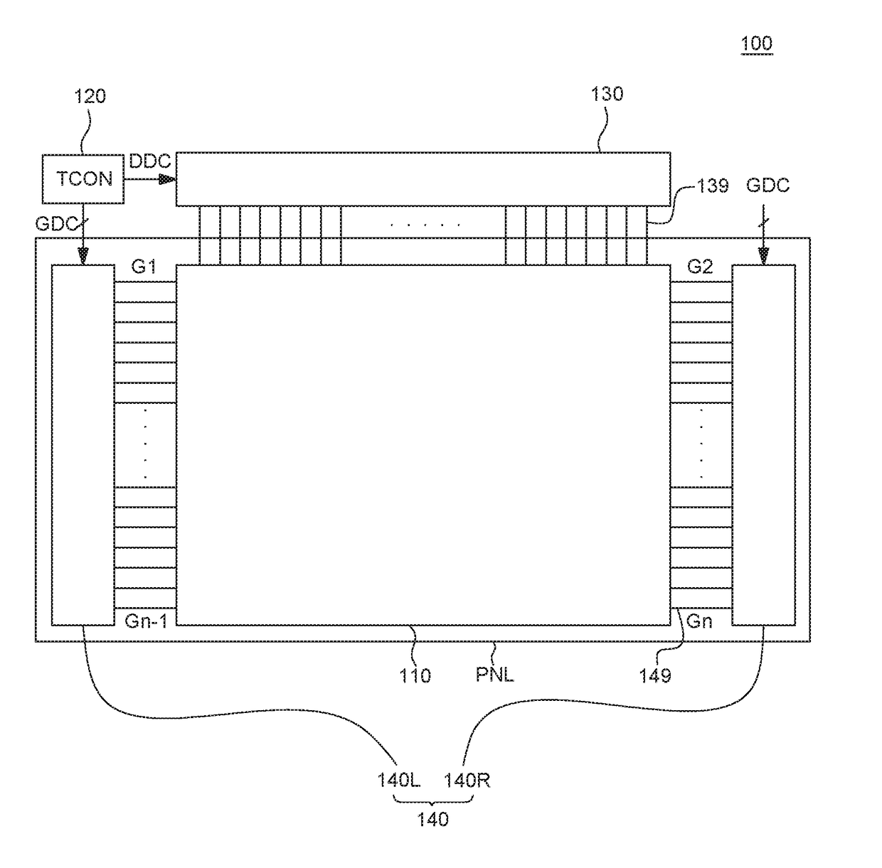
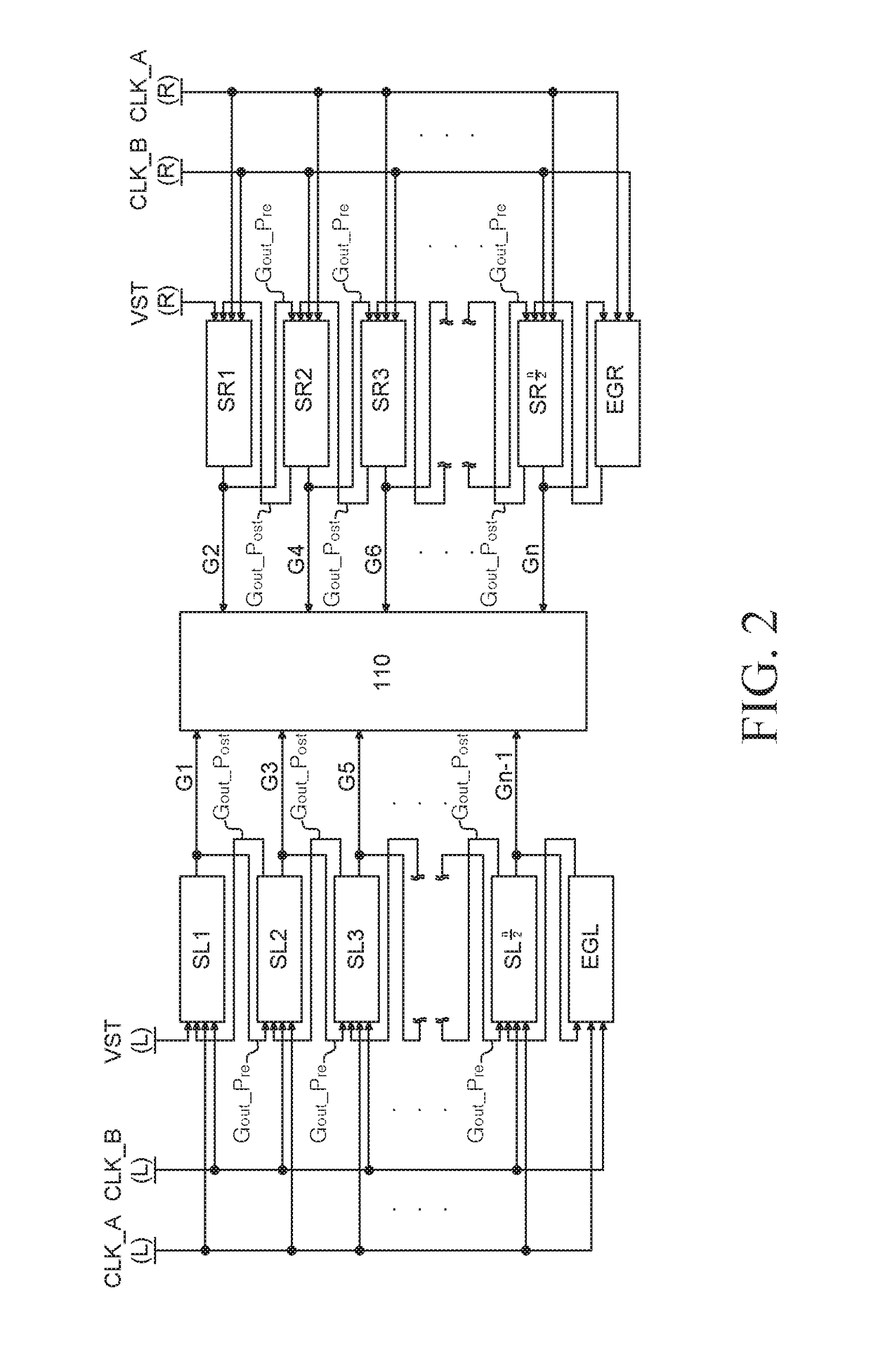
[0027]Advantages and features of the present disclosure, and methods for accomplishing the same will be more clearly understood from exemplary embodiments described below with reference to the accompanying drawings. However, the present disclosure is not limited to the following exemplary embodiments but may be implemented in various different forms. The exemplary embodiments are provided only to complete disclosure of the present disclosure and to fully provide a person having ordinary skill in the art to which the present disclosure pertains with the category of the disclosure, and the present disclosure will be defined by the appended claims.

[0028]The shapes, sizes, ratios, angles, numbers, and the like illustrated in the accompanying drawings for describing the exemplary embodiments of the present disclosure are merely examples, and the present disclosure is not limited thereto. Further, in the following description, a detailed explanation of known related technologies may be om...


PUM


Abstract

Provided are a gate driving circuit and a display device including the same. The gate driving circuit according to an embodiment includes a shift register including a plurality of stages. An nth stage of the stages includes a latch control circuit including a first NMOS transistor connected to a QB node, a second NMOS transistor connected to a Q node, and a third NMOS transistor having a gate electrode to which a first clock is input and connected to the first and second NMOS transistors, where n is a positive integer. A latch is connected between the Q and QB nodes. A transmission gate is connected to the Q and QB nodes. In the gate driving circuit, output signals of a previous stage and a following stage are controlled so as to be synchronized with the first clock to suppress a glitch.

Description

CROSS-REFERENCE TO RELATED APPLICATIONS[0001]This application claims the priority of Korean Patent Application No. 10-2015-0179281 filed on Dec. 15, 2015, in the Korean Intellectual Property Office, the disclosure of which is incorporated herein by reference.BACKGROUND[0002]Field[0003]The present disclosure relates to a gate driving circuit and a display device including the same, and more particularly, to a gate driving circuit capable of reducing glitches and a display device including the same.[0004]Description of the Related Art[0005]Flat panel displays (FPDs) have been employed in various electronic devices such as mobile phones, tablet PCs, notebook computers as well as televisions and monitors. Recently, for example, a liquid crystal display device (hereinafter, referred to as “LCD”) and an organic light emitting diode display (hereinafter, referred to as “OLED”) have been used as an FPD. Such a display device includes a plurality of pixels, a pixel array configured to displa...

Claims


Application Information

Patent Timeline
Patent Type & Authority Applications(United States)
IPC IPC(8): G09G3/20G11C19/28
CPCG09G3/2092G11C19/28G09G2310/0286G09G2300/043G09G2300/0819G09G2300/0809G09G2310/0291G09G3/20G09G3/3266G09G3/3677G09G2310/0264G09G2300/0408G09G2310/0267
Inventor KIM, BYUNGILCHOI, SEOKHWAN
Owner LG DISPLAY CO LTD
Why Eureka
Try Eureka