Semiconductor device and method of manufacturing semiconductor device

a semiconductor and semiconductor technology, applied in the direction of semiconductor devices, basic electric elements, electrical equipment, etc., can solve the problems of affecting device properties and complicated manufacturing steps, and achieve the effect of simplifying the number of manufacturing steps, simplifying the manufacturing steps, and affecting the properties of the devi

Active Publication Date: 2017-06-22
FUJI ELECTRIC CO LTD
View PDF0 Cites 7 Cited by
  • Summary
  • Abstract
  • Description
  • Claims
  • Application Information

AI Technical Summary

Benefits of technology

[0019]However, an edge termination structure in which areas of differing concentrations are nested therein is a microstructure, and thus requires a dry etching process each time a single region is formed, which complicates the manufacturing steps. Furthermore, an edge termination structure having a high concentration p-type region arranged in a ring shape in a low concentration p-type region narrows the allowable range of concentrations for p-type regions, which could greatly affect device properties due to variation in manufacturing steps. In addition, while an edge termination structure having a high concentration p-type region arranged in a ring shape in a low concentration p-type region does allow for the number of manufacturing steps to be simplified, such a structure narrows the acceptable amount of concentration variation for achieving high breakdown voltage.

Problems solved by technology

However, an edge termination structure in which areas of differing concentrations are nested therein is a microstructure, and thus requires a dry etching process each time a single region is formed, which complicates the manufacturing steps.
Furthermore, an edge termination structure having a high concentration p-type region arranged in a ring shape in a low concentration p-type region narrows the allowable range of concentrations for p-type regions, which could greatly affect device properties due to variation in manufacturing steps.

Method used


Image

  • Semiconductor device and method of manufacturing semiconductor device
  • Semiconductor device and method of manufacturing semiconductor device
  • Semiconductor device and method of manufacturing semiconductor device

Examples


embodiment 1

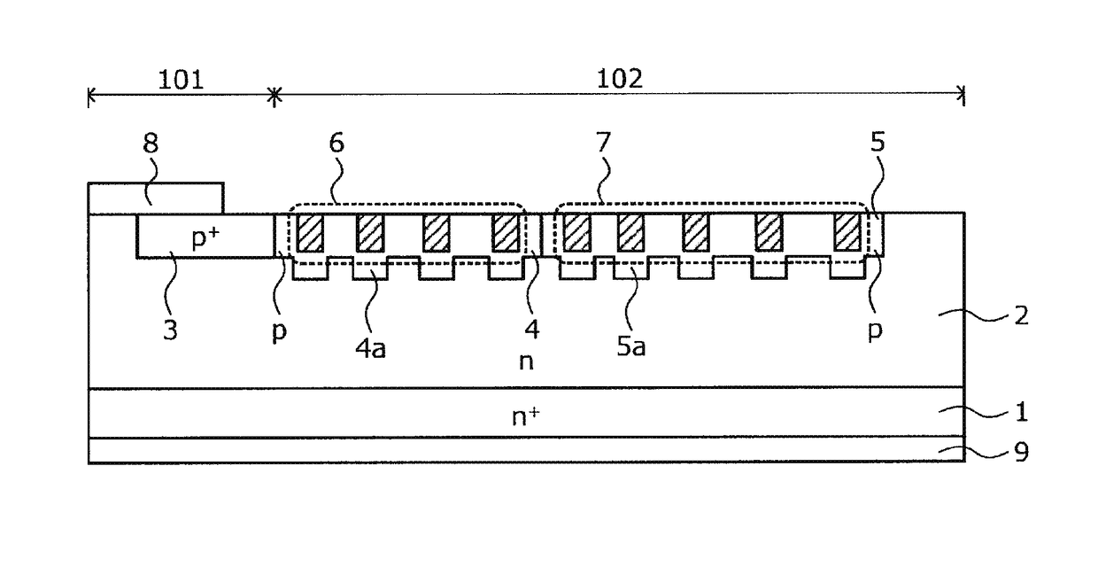
[0045]A semiconductor device in one aspect of the present invention is formed using a semiconductor with a wider bandgap than silicon (wide bandgap semiconductor). In Embodiment 1, a Schottky barrier diode (SBD) structure will be described as an example of a wide bandgap semiconductor such as a silicon carbide semiconductor device fabricated using silicon carbide (SiC).

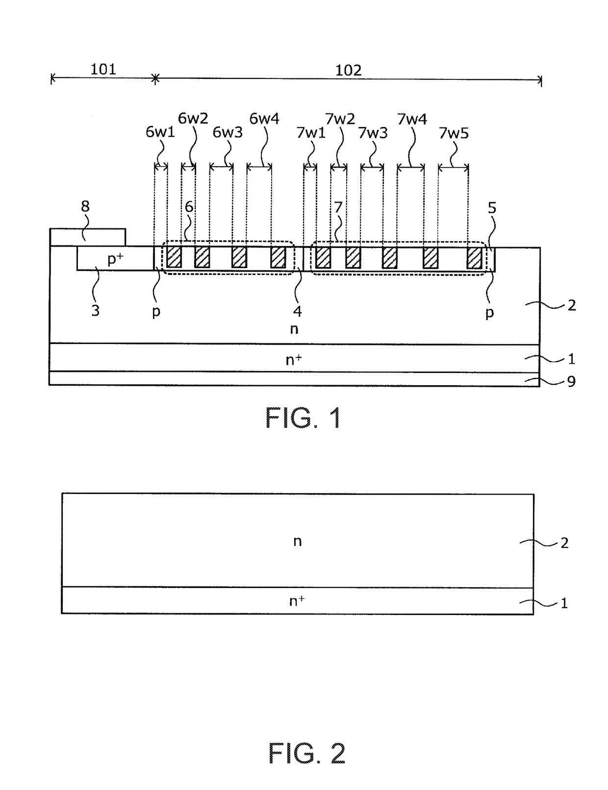
[0046]FIG. 1 is a cross-sectional view of a configuration of a silicon carbide semiconductor device according to Embodiment 1. As shown in FIG. 1, the silicon carbide semiconductor device of Embodiment 1 has a n-type silicon carbide epitaxial layer (a semiconductor deposited film of a first conductivity type) 2 deposited on a first primary surface (front surface) of an n30 silicon carbide substrate (a semiconductor substrate of the first conductivity type) 1, such as the (0001) surface (Si surface).

[0047]The n+ silicon carbide substrate 1 is a single-crystal silicon carbide substrate. The n-type silicon carbide epita...

embodiment 2

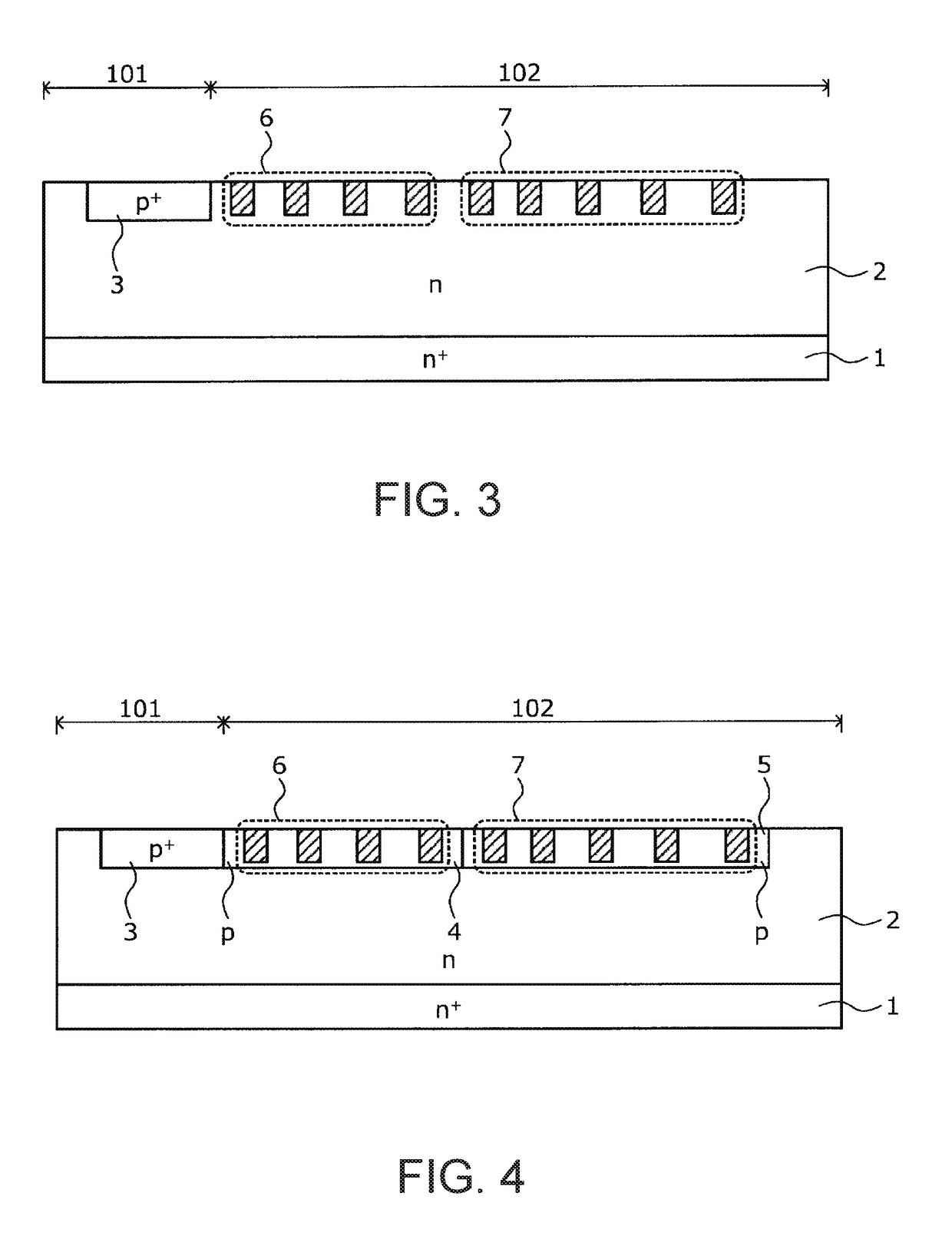
[0067]FIG. 5 is a cross-sectional view of a configuration of a silicon carbide semiconductor device according to Embodiment 2. As shown in FIG. 5, in the silicon carbide semiconductor device of Embodiment 2, the width of the first region of the plurality of fourth p-type regions 7 from the active region 101, or namely, the width of the fourth p-type region 7a, which is closest to the active region 101, is greater than the width of the other fourth p-type regions 7. Furthermore, the fourth p-type region 7a is formed at the border between the first p-type region 4 and the second p-type region 5.

[0068]The other configurations of the silicon carbide semiconductor device of Embodiment 2 are similar to the configurations of the silicon carbide semiconductor device of Embodiment 1, and thus overlapping explanations will be omitted.

[0069](Method of Manufacturing Semiconductor Device of Embodiment 2)

[0070]Next, a method of manufacturing a semiconductor device according to Embodiment 2 will b...

embodiment 3

[0074]FIG. 6 is a cross-sectional view of a configuration of a silicon carbide semiconductor device according to Embodiment 3. As shown in FIG. 3, in Embodiment 3, the thickness of a portion 4a of the first p-type region 4 overlapping the third p-type region 6 is greater than other portions of the first p-type region 4. Furthermore, the thickness of a portion 5a of the second p-type region 5 overlapping the fourth p-type region 7 is greater than other portions of the second p-type region 5. In other words, the portion 4a in the first p-type region 4 overlapping the third p-type region 6 is deeper than other portions of the first p-type region 4. In addition, the portion 5a in the second p-type region 5 overlapping the fourth p-type region 7 is deeper than other portions of the second p-type region 5.

[0075]The other configurations of the silicon carbide semiconductor device of Embodiment 3 are similar to the configurations of the silicon carbide semiconductor device of Embodiment 1, ...


PUM


Abstract

A semiconductor device includes an n+ type silicon carbide substrate, and in the substrate an active region where primary current flows and an edge termination area surrounding the active region. The semiconductor device has a first p-type region and a second p-type region in the edge termination area, and the first p-type region includes therein a plurality of third p-type regions, and the second p-type region includes therein a plurality of fourth p-type regions. The widths between the respective plurality of third p-type regions and the widths between the respective plurality of fourth p-type regions become greater further away from the active region.

Description

BACKGROUND OF THE INVENTION[0001]Technical Field[0002]The present invention relates to a semiconductor device and a method of manufacturing a semiconductor device.[0003]Background Art[0004]Silicon (Si) is conventionally used as the constituting material for power semiconductor devices, which control high voltages and large currents. There are several types of power semiconductor devices, such as bipolar or IGBTs (insulated gate bipolar transistors) and MOSFETs (metal oxide semiconductor field effect transistors), each specialized for different uses.[0005]For example, bipolar transistors or IGBTs have higher current density than MOSFETs and can have large currents, but cannot be switched at high speeds. Specifically, bipolar transistors are limited to switching frequencies of several kHz, and IGBTs are limited to switching frequencies of several dozen kHz. On the other hand, power MOSFETs have lower current density than bipolar transistors or IGBTs and cannot easily have large curren...

Claims


Application Information

Patent Timeline
Patent Type & Authority Applications(United States)
IPC IPC(8): H01L29/16H01L21/02H01L29/06H01L29/66H01L29/739H01L29/36
CPCH01L29/1608H01L29/7393H01L21/02529H01L29/0615H01L29/66325H01L29/36H01L29/0688H01L29/2003H01L29/6606H01L29/66712H01L29/7811H01L29/872
Inventor KINOSHITA, AKIMASA
Owner FUJI ELECTRIC CO LTD
Why Eureka
Try Eureka