Active layer, thin-film transistor array substrate comprising the same, and display device comprising the same
a technology of thin-film transistors and array substrates, applied in non-linear optics, instruments, optics, etc., can solve the problems of low on/off ratio and high cost of polycrystalline silicon in large-area electronics, and achieve the effect of improving device characteristics
Active Publication Date: 2017-06-29
LG DISPLAY CO LTD
View PDF11 Cites 3 Cited by
- Summary
- Abstract
- Description
- Claims
- Application Information
AI Technical Summary
Benefits of technology
The present invention provides an active layer that includes carbon allotropes, which improves device performance. This improved performance is achieved through the use of a thin-film transistor array substrate that includes the active layer, resulting in a display device with improved quality.
Problems solved by technology
Polycrystalline silicon has a high electron mobility of about 100 cm2 / Vs, but has a lower on / off ratio compared to oxide semiconductor and it costs a lot to apply polycrystalline silicon in large-area electronics.
Method used
View moreImage
Smart ImageViewing Examples

Examples
example
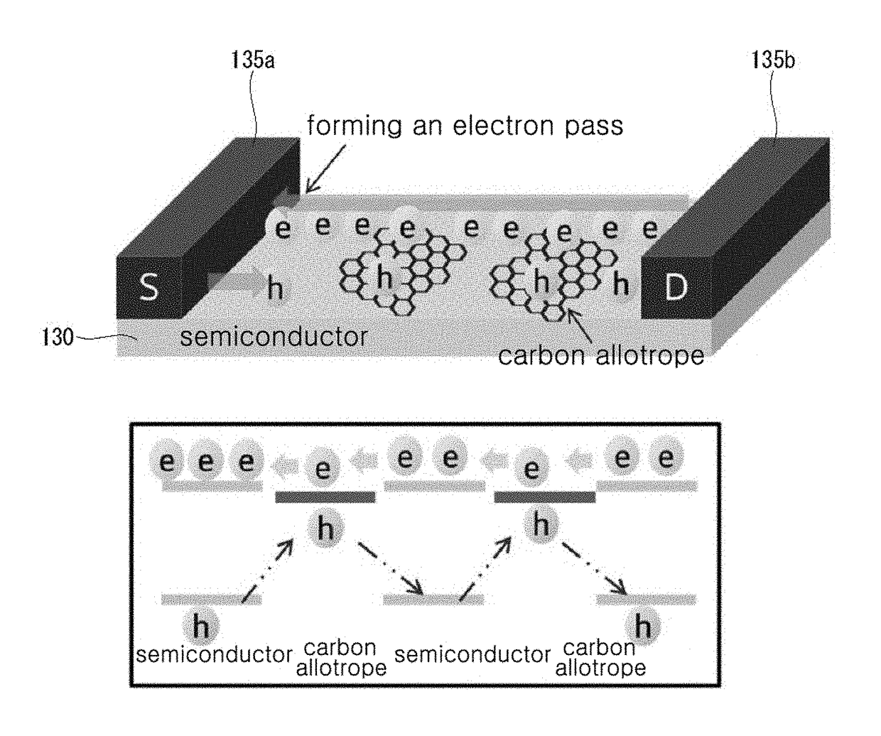
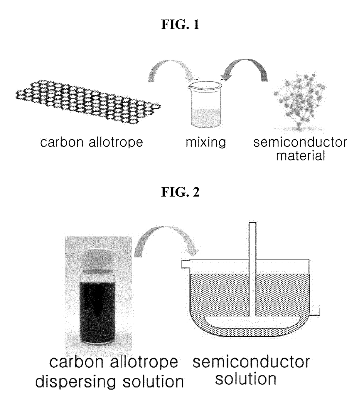
[0088]As shown above in FIG. 2, a thin-film transistor is made by forming an active layer comprising carbon allotropes and a semiconductor in a bottom-gate type thin-film transistor. The semiconductor material used is IGZO.
Login to View More PUM
| Property | Measurement | Unit |
|---|---|---|
| thickness | aaaaa | aaaaa |
| thickness | aaaaa | aaaaa |
| thickness | aaaaa | aaaaa |
Abstract
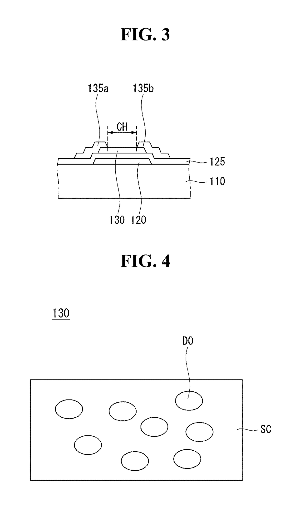
Carbon allotropes, a thin-film transistor array substrate comprising the same, and a display device comprising the same are disclosed. The thin-film transistor array substrate comprising a substrate, a gate electrode on the substrate, a gate insulating film on the gate electrode, an active layer positioned on the gate insulating film and comprising a semiconductor material and a plurality of carbon allotropes, and a source electrode and a drain electrode that make contact with the active layer.
Description
CROSS-REFERENCE TO RELATED APPLICATION[0001]This application claims the priority benefit of Korean Patent Application No. 10-2015-0187704 filed in the Republic of Korea on Dec. 28, 2015, which is incorporated herein by reference in its entirety for all purposes as if fully set forth herein.BACKGROUND[0002]Field of the Disclosure[0003]The present disclosure relates to a display device, and more particularly, to an active layer, a thin-film transistor array substrate comprising the same, and a display device comprising the same. Although the present disclosure is suitable for a wide scope of applications, it is particularly suitable for improving device characteristics of the display device by implementing an active layer formed of carbon allotropes.[0004]Description of the Background[0005]With the development of multimedia, flat panel displays (FDPs) are becoming more and more important nowadays. In line with this, a variety of flat panel displays such as liquid crystal displays (LCD...
Claims
Login to View More Application Information
Patent Timeline
 Patent Type & Authority Applications(United States)
IPC IPC(8): H01L27/12H01L29/267H01L29/786H01L27/28H01L27/32G02F1/1368H01L51/05H01L29/16
CPCH01L27/1222H01L51/0566H01L29/267H01L29/1606H01L27/1225G02F2202/10H01L27/3274G02F1/1368H01L29/78606H01L29/78684H01L27/283H01L29/12H10K59/12H01L29/78618H01L29/7869H01L29/78696H10K10/488H10K19/10H10K59/125
Inventor KANG, JIYEONKIM, CHANGEUNBAEK, JEONGEUNKIM, SUNGJIN
Owner LG DISPLAY CO LTD
Features
- R&D
- Intellectual Property
- Life Sciences
- Materials
- Tech Scout
- Unparalleled Data Quality
- Higher Quality Content
- 60% Fewer Hallucinations
Learn More Browse by: Latest US Patents, China's latest patents, Technical Efficacy Thesaurus, Application Domain, Technology Topic, Popular Technical Reports.
© 2025 PatSnap. All rights reserved.Legal|Privacy policy|Modern Slavery Act Transparency Statement|Sitemap|About US| Contact US: help@patsnap.com