
Power device on bulk substrate

a power device and bulk substrate technology, applied in the field of electromechanical circuits, can solve the problems of high product cost, and achieve the effect of improving the long-term reliability of the mosfet power device and reducing gate-to-drain capacitan

Active Publication Date: 2017-08-10
SILANNA ASIA
View PDF3 Cites 15 Cited by
  • Summary
  • Abstract
  • Description
  • Claims
  • Application Information

AI Technical Summary

Benefits of technology

The invention provides semiconductor structures and techniques that help integrate circuits and components on the same silicon substrate as control circuitry for a power control device. It also reduces gate-to-drain capacitance in MOSFET power devices and minimizes injection of hot carriers, improving the long-term reliability of the MOSFET power device.

Problems solved by technology

Consequently, an allocation of a large die area to the power switch leads to a high product cost, which is undesirable.

Method used


Image

  • Power device on bulk substrate
  • Power device on bulk substrate
  • Power device on bulk substrate

Examples


Embodiment Construction

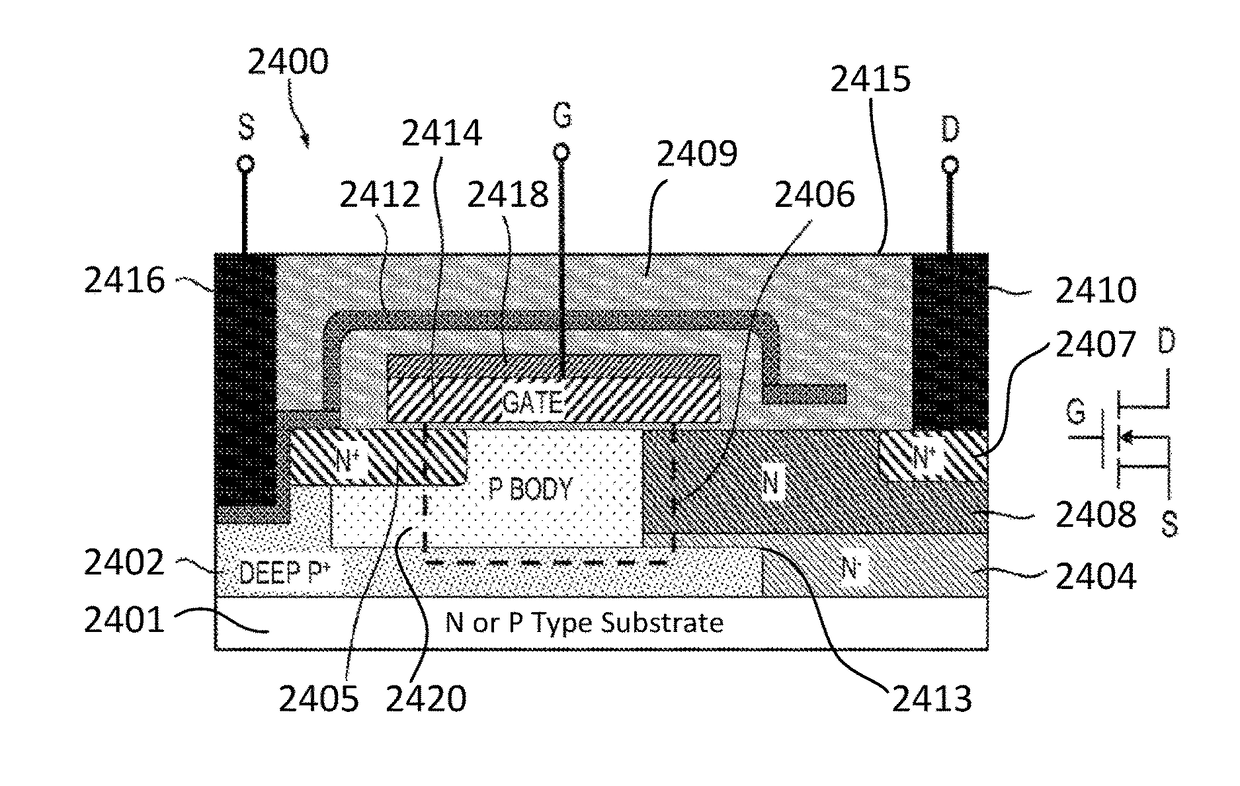
[0045]Embodiments of the invention will be described herein in the context of illustrative power management circuits and semiconductor fabrication methods for forming one or more components suitable for use in the illustrative power management circuits. It should be understood, however, that embodiments of the invention are not limited to the particular circuits and / or methods shown and described herein. Rather, embodiments of the invention are more broadly related to techniques for fabricating an integrated circuit in a manner which achieves high-frequency performance for a variety of power management applications, such as, for example, a DC / DC power converter, and advantageously reduces the physical size and cost of external components which may be used in conjunction with embodiments of the invention, such as, for example, an output filter, among other benefits. Moreover, it will become apparent to those skilled in the art given the teachings herein that numerous modifications ca...


PUM


Abstract

A metal-oxide-semiconductor field-effect transistor (MOSFET) power device includes an active region formed on a bulk semiconductor substrate, the active region having a first conductivity type formed on at least a portion of the bulk semiconductor substrate. A first terminal is formed on an upper surface of the structure and electrically connects with at least one other region having the first conductivity type formed in the active region. A buried well having a second conductivity type is formed in the active region and is coupled with a second terminal formed on the upper surface of the structure. The buried well and the active region form a clamping diode which positions a breakdown avalanche region between the buried well and the first terminal. A breakdown voltage of at least one of the power devices is a function of characteristics of the buried well.

Description

CROSS-REFERENCE TO RELATED APPLICATION(S)[0001]This patent application is a continuation-in-part of and claims the benefit of U.S. patent application Ser. No. 15 / 228,213 filed on Aug. 4, 2016, entitled “Power Device Integration on a Common Substrate”, which was a continuation of and claims the benefit of U.S. patent application Ser. No. 13 / 939,451 filed on Jul. 11, 2013, entitled “Power Device Integration on a Common Substrate”, which was a continuation-in-part of and claims the benefit of U.S. patent application Ser. No. 13 / 887,704 filed on May 6, 2013, entitled “Power Device Integration on a Common Substrate”, which claims priority to U.S. Provisional Patent Application Ser. No. 61 / 677,660 filed on Jul. 31, 2012, entitled “Power Management Integrated Circuit for Portable Electronic Devices,” the disclosure of each of which is incorporated herein by reference in its entirety for all purposes.FIELD OF THE INVENTION[0002]The present invention relates generally to electronic circuits,...

Claims


Application Information

Patent Timeline
IPC IPC(8): H01L29/06H01L29/78H01L29/73H01L29/739H01L29/10H01L29/872H01L29/8605H01L29/94H01L21/8249H01L29/49H01L29/40H01L29/861
CPCH01L29/0626H01L29/1095H01L29/7821H01L29/7824H01L29/7825H01L29/7302H01L29/7313H01L29/7391H01L29/8611H01L29/8725H01L29/8605H01L29/945H01L21/8249H01L29/4933H01L29/402H01L21/823437H01L27/0629H01L27/0635H01L27/088H01L29/0688H01L29/1008H01L29/1083H01L29/1087H01L29/36H01L29/41766H01L29/42304H01L29/4236H01L29/66181H01L29/6625H01L29/66265H01L29/66659H01L29/66681H01L29/66696H01L29/66704H01L29/7317H01L29/735H01L29/7835H01L29/861H01L29/872H01L2224/0401H01L2224/05569H01L2224/05572H01L2224/11H01L2224/13H01L2924/00014H01L2924/12032H01L2924/1305H01L2924/13062H01L2924/13091H01L2924/00H01L2224/05552
Inventor STUBER, MICHAEL A.MOLIN, STUART B.KOREC, JACEKYANG, BOYI
Owner SILANNA ASIA
Learn More